
- Manufacturer Part Number : AD5592RBCBZ-RL7
- Manufacturer : AD
- Description : 8 Channel, 12-Bit, Configurable ADC/DAC with on-chip Reference, SPI interface IC
- Series : AD5592R
- Reference Price : USD 2.6
- Our Price : We have a better price, contact us by email
- Product Type : Integrated/Special Purpose A/D Converters
- Function : A/D & D/A Converter Combinations
- Current Suggest : Recommended for New Designs
- Status : Production
- ROHS Status : ROHS Compliant (Lead Free)
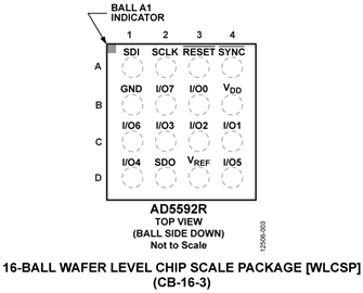
- Package Type : 16-Ball WLCSP (1.96mm x 1.96mm)
- Pins : 16
- MFG Package Case : CB-16-3
- Part Type : REEL
- Standard Packing Type : Reel
- Standard Packing Quantity : 3000
- Working Temperature : -40 to 105C
- Other Part Number : AD5592RBCBZ-RL7
- Shipping methods : DHL FEDEX UPS TNT
- Delivery Time : Ship within 1 day.
- Manufacturer Production time : 6-8 weeks (Normally have stocks)
- Weight : 0.001KG
Contact us to check the best price and real time inventory quantity for AD5592RBCBZ-RL7. If you need any more information about AD5592RBCBZ-RL7, you can also send us by email. Our email is [email protected], we will reply you in 12 hours.
- Download AD5592R-1-KGD Data Sheet. Available as Known Good Die and fully guaranteed to data sheet specifications.
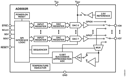
- 8-channel, configurable ADC/DAC/GPIO
- Configurable as any combination of
- 8 × 12-bit DAC channels
- 8 × 12-bit ADC channels
- 8 × general-purpose digital input/output pins
- Integrated temperature sensor
- SPI interface
- Available in
- 16-ball, 2 mm × 2 mm WLCSP
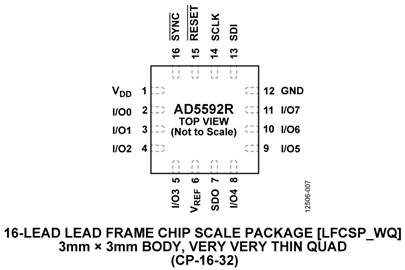
- 16-lead, 3 mm × 3 mm LFCSP
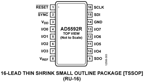
- 16-lead TSSOP
The AD5592R/AD5592R-1 have eight I/Ox pins (I/O0 to I/O7) that can be independently configured as digital-to-analog converter (DAC) outputs, analog-to-digital converter (ADC) inputs, digital outputs, or digital inputs. When an I/Ox pin is configured as an analog output, it is driven by a 12-bit DAC. The output range of the DAC is 0 V to VREF or 0 V to 2 × VREF.
When an I/Ox pin is configured as an analog input, it is connected to a 12-bit ADC via an analog multiplexer. The input range of the ADC is 0 V to VREF or 0 V to 2 × VREF. The ADC has a total throughput rate of 400 kSPS. The I/Ox pins can also be configured as digital, general-purpose input or output (GPIO) pins. The state of the GPIO pins can be set or read back by accessing the GPIO write data register or the GPIO read configuration register, respectively, via a serial peripheral interface (SPI) write or read operation.
The AD5592R/AD5592R-1 have an integrated 2.5 V, 25 ppm/°C reference, which is turned off by default, and an integrated temperature indicator, which gives an indication of the die temperature. The temperature value is read back as part of an ADC read sequence.
The AD5592R/AD5592R-1 are available in 16-ball, 2 mm × 2 mm WLCSP, 16-lead, 3 mm × 3 mm LFCSP, and 16-lead TSSOP. The AD5592R/AD5592R-1 operate over a temperature range of −40°C to +105°C.
Applications
- Control and monitoring
- General-purpose analog and digital inputs/outputs
This product has been released to the market. The data sheet contains all final specifications and operating conditions. For new designs, ADI recommends utilization of these products.
