
- Manufacturer Part Number : AD6641BCPZRL7-500
- Manufacturer : AD
- Description : 250 MHz Bandwidth DPD Observation Receiver IC
- Series : AD6641
- Reference Price : USD 99.96
- Our Price : We have a better price, contact us by email
- Product Type : High Speed A/D Converters >10 MSPS
- Function : IF/RF Receivers
- Current Suggest : Recommended for New Designs
- Status : Production
- ROHS Status : ROHS Compliant (Lead Free)
- Package Type : 56-Lead LFCSP (8mm x 8mm)
- Pins : 56
- MFG Package Case : CP-56-1
- Part Type : REEL
- Standard Packing Type : Reel
- Standard Packing Quantity : 750
- Working Temperature : -40 to 85C
- Other Part Number : AD6641BCPZRL7-500
- Shipping methods : DHL FEDEX UPS TNT
- Delivery Time : Ship within 1 day.
- Manufacturer Production time : 6-8 weeks (Normally have stocks)
- Weight : 0.001KG
Contact us to check the best price and real time inventory quantity for AD6641BCPZRL7-500. If you need any more information about AD6641BCPZRL7-500, you can also send us by email. Our email is [email protected], we will reply you in 12 hours.
- SNR = 65.8 dBFS at fIN up to 250MHz at 500 MSPS
- ENOB of 10.5 at fIN up to 250 MHz at 500 MSPS (−1.0 dBFS)
- SFDR = 80 dBc at fIN up to 250 MHz at 500 MSPS (−1.0 dBFS)
- Excellent linearity
DNL = ±0.5 LSB typical,
INL = ±0.6 LSB typical - Integrated 16k × 12 FIFO
- FIFO readback options
12-bit CMOS at 62.5MHz
6-bit DDR LVDS interface
SPORT at 62.5 MHz
SPI at 25MHz - High speed synchronization capability
- 1 GHz full power analog bandwidth
- Integrated input buffer
- On-chip reference, no external decoupling required
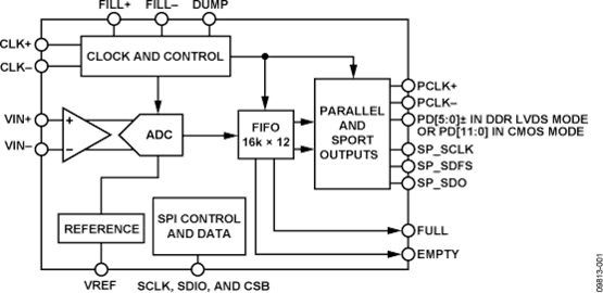
The AD6641 is a 250 MHz bandwidth digital predistortion observation receiver that integrates a 12-bit 500 MSPS ADC, a 16k × 12 FIFO, and a multimode back end that allows users to retrieve the data through a serial port (SPORT), the SPI interface, or a 12-bit parallel CMOS or 6-bit DDR LVDS port after being stored in the integrated FIFO memory. It is optimized for outstanding dynamic performance and low power consumption and is suitable for use in telecommunications applications such as a digital predistortion observation path where wider bandwidths are desired. All necessary functions, including the sample-and-hold, and voltage reference are included on the chip to provide a complete signal conversion solution.
The on-chip FIFO allows for small snapshots of time to be captured via the ADC and read back at a lower rate. This reduces the constraints of signal processing by transferring the captured data at an arbitrary time and at a much lower sample rate. The FIFO can be operated in several user programmable modes. In the single capture mode, the ADC data is captured when signaled via the SPI port or the use of the external FILL± pins. In the continuous capture mode, the data is loaded constantly into the FIFO and the FILL± pins are used to stop this operation.
APPLICATIONS
- Wireless and wired broadband communications
- Communications test equipment
- Power amplifier linearization
This product has been released to the market. The data sheet contains all final specifications and operating conditions. For new designs, ADI recommends utilization of these products.


