
- Manufacturer Part Number : AD6642BBCZ
- Manufacturer : AD
- Description : Dual IF Receiver IC
- Series : AD6642
- Reference Price : USD 60.68
- Our Price : We have a better price, contact us by email
- Product Type : Integrated/Special Purpose A/D Converters
- Function : IF/RF Receivers
- Current Suggest : Production
- Status : Production
- ROHS Status : ROHS Compliant (Lead Free)
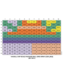
- Package Type : 144-Ball CSPBGA (10mm x 10mm x 1.4mm)
- Pins : 144
- MFG Package Case : BC-144-1
- Part Type : OTH
- Standard Packing Type : Tray
- Standard Packing Quantity : 184
- Working Temperature : -40 to 85C
- Other Part Number : AD6642BBCZ
- Shipping methods : DHL FEDEX UPS TNT
- Delivery Time : Ship within 1 day.
- Manufacturer Production time : 6-8 weeks (Normally have stocks)
- Weight : 0.001KG
Contact us to check the best price and real time inventory quantity for AD6642BBCZ. If you need any more information about AD6642BBCZ, you can also send us by email. Our email is [email protected], we will reply you in 12 hours.
- 11-bit, 200 MSPS output data rate per channel
- Integrated noise shaping requantizer (NSR)
- Performance with NSR enabled
SNR: 75.5 dBFS in 40 MHz band to 70 MHz @ 185 MSPS
SNR: 73.7 dBFS in 60 MHz band to 70 MHz @ 185 MSPS - Performance with NSR disabled
SNR: 66.5 dBFS to 70 MHz @ 185 MSPS
SFDR: 83 dBc to 70 MHz @ 185 MSPS - Low power: 0.62 W @ 185 MSPS
- 1.8 V analog supply operation
- 1.8 V LVDS (ANSI-644 levels) output
- 1-to-8 integer clock divider
- Internal ADC voltage reference
- 1.75 V p-p analog input range
(programmable to 2.0 V p-p) - Differential analog inputs with 800 MHz bandwidth
- See data sheet for additional features
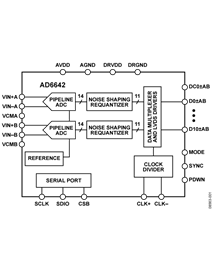
The AD6642 is an 11-bit, 200 MSPS, dual-channel intermediate frequency (IF) receiver specifically designed to support multi-antenna systems in telecommunication applications where high dynamic range performance, low power, and small size are desired.
The device consists of two high performance analog-to-digital converters (ADCs) and noise shaping requantizer (NSR) digital blocks. Each ADC consists of a multistage, differential pipelined architecture with integrated output error correction logic. The ADC features a wide bandwidth switched-capacitor sampling network within the first stage of the differential pipeline. An integrated voltage reference eases design considerations. A duty cycle stabilizer (DCS) compensates for variations in the ADC clock duty cycle, allowing the converters to maintain excellent performance.
Each ADC output is connected internally to an NSR block. The integrated NSR circuitry allows for improved SNR performance in a smaller frequency band within the Nyquist bandwidth. The device supports two different output modes selectable via the external MODE pin or the SPI.
With the NSR feature enabled, the outputs of the ADCs are processed such that the AD6642 supports enhanced SNR performance within a limited portion of the Nyquist bandwidth while maintaining an 11-bit output resolution. The NSR block can be programmed to provide a bandwidth of either 22% or 33% of the sample clock. For example, with a sample clock rate of 185 MSPS, the AD6642 can achieve up to 75.5 dBFS SNR for a 40 MHz bandwidth in the 22% mode and up to 73.7 dBFS SNR for a 60 MHz bandwidth in the 33% mode.
With the NSR block disabled, the ADC data is provided directly to the output with a resolution of 11 bits. The AD6642 can achieve up to 66.5 dBFS SNR for the entire Nyquist bandwidth when operated in this mode. This allows the AD6642 to be used in telecommunication applications such as a digital predistortion observation path where wider bandwidths are desired.
After digital signal processing, multiplexed output data is routed into two 11-bit output ports such that the maximum data rate is 400 Mbps (DDR). These outputs are set at 1.8 V LVDS and support ANSI-644 levels.The AD6642 receiver digitizes a wide spectrum of IF frequencies. Each receiver is designed for simultaneous reception of a separate antenna. This IF sampling architecture greatly reduces compo-nent cost and complexity compared with traditional analog techniques or less integrated digital methods.
Flexible power-down options allow significant power savings. Programming for device setup and control is accomplished using a 3-wire SPI-compatible serial interface with numerous modes to support board-level system testing.The AD6642 is available in a Pb-free/RoHS compliant, 144-ball, 10 mm × 10 mm chip scale package ball grid array (CSP_BGA) and is specified over the industrial temperature range of −40°C to +85°C.
Applications
- Communications
- Diversity radio and smart antenna (MIMO) systems
- Multimode digital receivers (3G)
- WCDMA, LTE, CDMA2000
- WiMAX, TD-SCDMA
- I/Q demodulation systems
- General-purpose software radios
At least one model within this product family is in production and available for purchase. The product is appropriate for new designs but newer alternatives may exist.


