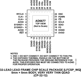

- Manufacturer Part Number : AD6677BCPZ
- Manufacturer : AD
- Description : 80 MHz Bandwidth, IF Receiver IC
- Series : AD6677
- Reference Price : USD 35.36
- Our Price : We have a better price, contact us by email
- Product Type : Integrated/Special Purpose A/D Converters
- Function : IF/RF Receivers
- Current Suggest : Recommended for New Designs
- Status : Production
- ROHS Status : ROHS Compliant (Lead Free)
- Package Type : 32-Lead LFCSP (5mm x 5mm x 0.75mm w/ EP)
- Pins : 32
- MFG Package Case : CP-32-12
- Part Type : OTH
- Standard Packing Type : Tray
- Standard Packing Quantity : 490
- Working Temperature : -40 to 85C
- Other Part Number : AD6677BCPZ
- Shipping methods : DHL FEDEX UPS TNT
- Delivery Time : Ship within 1 day.
- Manufacturer Production time : 6-8 weeks (Normally have stocks)
- Weight : 0.001KG
Contact us to check the best price and real time inventory quantity for AD6677BCPZ. If you need any more information about AD6677BCPZ, you can also send us by email. Our email is [email protected], we will reply you in 12 hours.
- JESD204B Subclass 0 or Subclass 1 coded serial digital outputs
- Signal-to-noise ratio (SNR) = 71.9 dBFS at 185 MHz AIN and 250 MSPS with NSR set to 33%
- Spurious-free dynamic range (SFDR) = 87 dBc at 185 MHz AIN and 250 MSPS
- Total power consumption:
435 mW at 250 MSPS - 1.8 V supply voltages
- Integer 1 to 8 input clock divider
- Sample rates of up to 250 MSPS
- IF sampling frequencies of up to 400 MHz
- Internal analog-to-digital converter (ADC) voltage reference
- Flexible analog input range
1.4 V p-p to 2.0 V p-p (1.75 V p-p nominal) - ADC clock duty cycle stabilizer (DCS)
- Serial port control
- Energy saving power-down modes
The AD6677 is an 11-bit, 250 MSPS, intermediate frequency(IF) receiver specifically designed to support multi-antennasystems in telecommunication applications where high dynamicrange performance, low power, and small size are desired.
The device consists of a high performance analog-to-digitalconverter (ADC) and a noise shaping requantizer (NSR) digitalblock. The ADC consists of a multistage, differential pipelinedarchitecture with integrated output error correction logic, andeach ADC features a wide bandwidth switched capacitor samplingnetwork within the first stage of the differential pipeline. Anintegrated voltage reference eases design considerations. A dutycycle stabilizer (DCS) compensates for variations in the ADCclock duty cycle, allowing the converters to maintain excellentperformance.
The ADC output is connected internally to an NSR block. Theintegrated NSR circuitry allows for improved SNR performancein a smaller frequency band within the Nyquist bandwidth. Thedevice supports two different output modes selectable via theSPI. With the NSR feature enabled, the output of the ADCare processed such that the AD6677 supports enhanced SNRperformance within a limited portion of the Nyquist bandwidthwhile maintaining an 11-bit output resolution.
The NSR block can be programmed to provide a bandwidth ofeither 22% or 33% of the sample clock. For example, with a sampleclock rate of 250 MSPS, the AD6677 can achieve up to 76.3 dBFSSNR for a 55 MHz bandwidth in the 22% mode and up to73.5 dBFS SNR for a 82 MHz bandwidth in the 33% mode.
When the NSR block is disabled, the ADC data is provided directlyto the output at a resolution of 11 bits. The AD6677 can achieveup to 65.9 dBFS SNR for the entire Nyquist bandwidth whenoperated in this mode. This allows the AD6677 to be used intelecommunication applications such as a digital predistortionobservation path where wider bandwidths are required.
The output data is routed directly to an external JESD204B serialoutput lane. This output is at current mode logic (CML) voltagelevels. One mode is supported such that the output coded data issent through one lane (L = 1; F = 4). Synchronization inputcontrols (SYNCINB± and SYSREF±) are provided.
The AD6677 receiver digitizes a wide spectrum of IF frequencies.This IF sampling architecture greatly reduces component cost andcomplexity compared with traditional analog techniques or lessintegrated digital methods.
Flexible power-down options allow significant power savings,when desired. Programmable overrange level detection issupported via dedicated fast detect pins.
Product Highlights
- The configurable JESD204B output block with an integrated phase-locked loop (PLL) to support lane rates up to 5 Gbps.
- IF receiver includes an 11-bit, 250 MSPS ADC with programmable noise shaping requantizer (NSR) function that allows for improved SNR within a reduced bandwidth of 22% or 33% of the sample rate.
- Support for an optional RF clock input to ease system board design.
- Proprietary differential input maintains excellent SNR performance for input frequencies of up to 400 MHz.
- An on-chip integer, 1 to 8 input clock divider and SYNC input allows synchronization of multiple devices.
- Operation from a single 1.8 V power supply.
- Standard serial port interface (SPI) that supports various product features and functions, such as controlling the clock DCS, power-down, test modes, voltage reference mode, overrange fast detection, and serial output configuration.
Applications
- Communications
- Diversity radio and smart antenna (MIMO) systems
- Multimode digital receivers (3G)
TD-SCDMA, WiMAX, WCDMA,
CDMA2000, GSM, EDGE, LTE - I/Q demodulation systems
- General-purpose software radios
This product has been released to the market. The data sheet contains all final specifications and operating conditions. For new designs, ADI recommends utilization of these products.


