Best Price NOW
Manufacturer / Brand: AD
Details: DC to 204 kHz, Dynamic Signal Analysis, Precision 24-Bit ADC with Power Scaling
Series: AD7768-1
Quantity Available: Over 11730 pieces
Product Parameters
- Manufacturer Part Number : AD7768-1
- Manufacturer : AD
- Description : DC to 204 kHz, Dynamic Signal Analysis, Precision 24-Bit ADC with Power Scaling
- Series : AD7768-1
- Reference Price : USD 4.76
- Our Price : We have a better price, contact us by email
- Product Type : Precision A/D Converters
- Function : Single Channel A/D Converters
- Current Suggest : Recommended for New Designs
- Status : Production
- RoHS Status: -
- Voltage: -
- Feature: -
- Package Case: -
- Temperature Range: -
- Packing: Reel/Tray/Tube
- Standard Packing Quantity: -
- Country of Origin: -
- Other Part Number : AD7768-1
- Shipping methods : DHL FEDEX UPS TNT
- Delivery Time : Ship within 1 day.
- Manufacturer Production time : 6-8 weeks (Normally have stocks)
- Weight : 0.001KG
Contact us to check the best price and real time inventory quantity for AD7768-1. If you need any more information about AD7768-1, you can also send us by email. Our email is [email protected], we will reply you in 12 hours.
Features and Benefits of AD7768-1
- ADC for single-channel low power, platform DAQ designs
- Wide bandwidth
- Sinc filter bandwidth range: DC to 204 kHz
- Low ripple FIR bandwidth range: DC to 110.8 kHz
- Precision ac and dc performance
- 108.5 dB dynamic range typical
- −120 dB THD
- ±1.1 ppm of FSR INL, ±30 µV offset error, ±30 ppm of FSR gain error
- Programmable ODR, filter type, and latency
- ODR values up to 1024 kSPS
- Linear phase digital filter options
- Low ripple FIR filter: ±0.005 dB maximum pass-band ripple, dc to 102.4 kHz
- Low latency sinc5 filter
- Low latency sinc3 filter enabling 50 Hz/60 Hz rejection
- Programmable FIR filter option
- Programmable power consumption and bandwidth
- Fast, highest speed
- 52.224 kHz bandwidth, 26.4 mW (sinc5 filter)
- 110.8 kHz bandwidth, 36.8 mW (FIR filter)
- Median, half speed: 55.4 kHz bandwidth, 19.7 mW (FIR filter)
- Low power, low speed: 13.9 kHz bandwidth, 6.75 mW (FIR filter)
- Power supply
- AVDD1 − AVSS = 5.0 V typical
- AVDD2 − AVSS = 2.0 V to 5.0 V typical
- Analog supplies can run from split supply (true bipolar)
- IOVDD − DGND = 1.8 V to 3.3 V typical
- Low power mode can run from single 3.0 V supply
- Pin control or SPI interface configurable
- Suite of diagnostic check mechanisms
- Temperature, interface CRC, and memory map CRC
- Package: 28-lead, 4 mm × 5 mm, LFCSP
- Temperature range: −40°C to +125°C
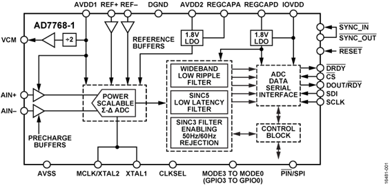
The AD7768-1 is a low power, high performance, Σ-Δ analog-to-digital converter (ADC), with a Σ-Δ modulator and digitalfilter for precision conversion of both ac and dc signals. The AD7768-1 is a single-channel version of the AD7768, an 8-channel, simultaneously sampling, Σ-Δ ADC. The AD7768-1 provides a single configurable and reusable data acquisition (DAQ) footprint, which establishes a new industry standard in combined ac and dc performance and enables instrumentation and industrial system designers to design across multiple measurement variants for both isolated and nonisolated applications.
The AD7768-1 achieves a 108.5 dB dynamic range when using the low ripple, finite impulse response (FIR) digital filter at 256 kSPS, giving 110.8 kHz input bandwidth, combined with ±1.1 ppm integral nonlinearity (INL), ±30 µV offset error, and ±30 ppm gain error.
A wider bandwidth, up to 500 kHz Nyquist (filter −3 dB point of 204 kHz), is available using the sinc5 filter, enabling a view of signals over an extended range.
The AD7768-1 offers the user the flexibility to configure and optimize for input bandwidth vs. output data rate (ODR) and vs. power dissipation. The flexibility of the AD7768-1 allows dynamic analysis of a changing input signal, making the device particularly useful in general-purpose DAQ systems. The selection of one of three available power modes allows the designer to achieve required noise targets while minimizing power consumption. The design of the AD7768-1 is unique in that it becomes a reusable and flexible platform for low power dc and high performance ac measurement modules.
The AD7768-1 achieves the optimum balance of dc and ac performance with excellent power efficiency. The following three operating modes allow the user to trade off the input bandwidth vs. power budgets:
- Fast mode offers both a sinc filter with up to 256 kSPS and 52.2 kHz of bandwidth, and 26.4 mW of power consumption, or a FIR filter with up to 256 kSPS, 110.8 kHz of bandwidth and 36.8 mW of power consumption.
- Median mode offers a FIR filter with up to 128 kSPS, 55.4 kHz of bandwidth and 19.7 mW of power consumption.
- Low power mode offers a FIR filter with up to 32 kSPS, 13.85 kHz of bandwidth and 6.75 mW of power consumption.
The AD7768-1 offers extensive digital filtering capabilities that meet a wide range of system requirements. The filter options allow configuration for frequency domain measurements with tight gain error over frequency, linear phase response requirements (brick wall filter), a low latency path (sinc5 or sinc3) for use in control loop applications, and measuring dc inputs with the ability to configure the sinc3 filter to reject the line frequency of either 50 Hz or 60 Hz. All filters offer programmable decimation.
A 1.024 MHz sinc5 filter path exists for users seeking an even higher ODR than is achievable using the low ripple FIR filter. This path is quantization noise limited. Therefore, it is best suited for customers requiring minimum latency for control loops or implementing custom digital filtering on an external field programmable gate array (FPGA) or digital signal processor (DSP).
The filter options include the following:
- A low ripple FIR filter with a ±0.005 dB pass-band ripple to 102.4 kHz.
- A low latency sinc5 filter with up to a 1.024 MHz data rate to maximize control loop responsiveness.
- A low latency sinc3 filter that is fully programmable, with 50 Hz/60 Hz rejection capabilities.
When using the AD7768-1, embedded analog functionalitywithin the AD7768-1 greatly reduces the design burden over theentire application range. The precharge buffer on each analoginput decreases the analog input current compared tocompeting products, simplifying the task of an externalamplifier to drive the analog input.
A full buffer input on the reference reduces the input current,providing a high impedance input for the external referencedevice or in buffering any reference sense resistor scenariosused in ratiometric measurements.
The device operates with a 5.0 V AVDD1 − AVSS supply, a 2.0 V to 5.0 V AVDD2 − AVSS supply, and a 1.8 V to 3.3 V IOVDD − DGND supply.
In low power mode, the AVDD1, AVDD2, and IOVDD supplies can run from a single 3.0 V rail.
The device requires an external reference. The absolute input reference (REFIN) voltage range is 1 V to AVDD1 − AVSS.
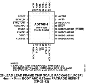
The specified operating temperature range is −40°C to +125°C. The device is housed in a 4 mm × 5 mm, 28-lead LFCSP.
Note that, throughout this data sheet, multifunction pins, suchas XTAL2/MCLK, are referred to either by the entire pin nameor by a single function of the pin, for example, MCLK, whenonly that function is relevant.
Applications
- Platform ADC to serve a superset of measurements and sensor types
- Sound and vibration, acoustic, and material science research and development
- Control and hardware in loop verification
- Condition monitoring for predictive maintenance
- Electrical test and measurement
- Audio testing and current and voltage measurement
- Clinical electroencephalogram (EEG), electromyogram (EMG), and electrocardiogram (ECG) vital signs monitoring
- USB-, PXI-, and Ethernet-based modular DAQ
- Channel to channel isolated modular DAQ designs


