
- Manufacturer Part Number : AD7779ACPZ
- Manufacturer : AD
- Description : 8-Channel, 24-Bit, Simultaneous Sampling ADC IC
- Series : AD7779
- Reference Price : USD 4.92
- Our Price : We have a better price, contact us by email
- Product Type : Precision A/D Converters
- Function : Simultaneous Sampling A/D Converters
- Current Suggest : Recommended for New Designs
- Status : Production
- ROHS Status : ROHS Compliant (Lead Free)
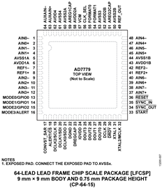
- Package Type : 64-Lead LFCSP (9mm x 9mm w/ EP)
- Pins : 64
- MFG Package Case : CP-64-15
- Part Type : OTH
- Standard Packing Type : Tray
- Standard Packing Quantity : 260
- Working Temperature : -40 to 125C
- Other Part Number : AD7779ACPZ
- Shipping methods : DHL FEDEX UPS TNT
- Delivery Time : Ship within 1 day.
- Manufacturer Production time : 6-8 weeks (Normally have stocks)
- Weight : 0.001KG
Contact us to check the best price and real time inventory quantity for AD7779ACPZ. If you need any more information about AD7779ACPZ, you can also send us by email. Our email is [email protected], we will reply you in 12 hours.
- 8-channel, 24-bit simultaneous sampling analog-to-digital converter (ADC)
- Single-ended or true differential inputs
- Programmable gain amplifier (PGA) per channel (gains of 1, 2, 4, and 8)
- Low dc input current
- ±1.5 nA (differential)
- ±4 nA (single-ended)
- Up to 16 kSPS output data rate (ODR) per channel
- Programmable ODRs and bandwidth
- Sample rate converter (SRC) for coherent sampling
- Sampling rate resolution up to 15.2 µSPS
- Low latency sinc3 filter path
- Adjustable phase synchronization
- Internal 2.5 V reference
- Two power modes optimizing power dissipation and performance: high resolution mode and low power mode
- Low resolution successive approximation (SAR) ADC for system and chip diagnostics
- Power supply
- Bipolar (±1.65 V) or unipolar (3.3 V) supplies
- Digital input/output (I/O) supply: 1.8 V to 3.6 V
- Performance temperature range: –40°C to +105°C
- Functional temperature range: –40°C to +125°C
- Performance
- Combined ac and dc performance
- 108 dB signal-to-noise ratio (SNR)/dynamic range at 16 kSPS in high resolution mode
- −109 dB total harmonic distortion (THD)
- ±7 ppm integral nonlinearity (INL)
- ±40 µV offset error
- ±0.1% gain error±10 ppm/°C typical temperature coefficient
- ±10 ppm/°C typical temperature coefficient
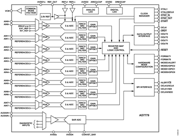
The AD7779 is an 8-channel, simultaneous sampling ADC.There are eight full Σ-Δ ADCs on chip. The AD7779 providesan ultralow input current to allow direct sensor connection. Eachinput channel has a programmable gain stage allowing gains of1, 2, 4, and 8 to map lower amplitude sensor outputs into thefull-scale ADC input range, maximizing the dynamic range ofthe signal chain. The AD7779 accepts VREF from 1 V up to 3.6 V.The analog inputs accept unipolar (0 V to VREF/GAIN) or truebipolar (±VREF/GAIN/2 V) analog input signals with 3.3 V or±1.65 V analog supply voltages. The analog inputs can beconfigured to accept true differential, pseudo differential, or singleendedsignals to match different sensor output configurations.
Each channel contains an ADC modulator and a sinc3, lowlatency digital filter. An SRC is provided to allow fine resolutioncontrol over the AD7779 ODR. This control can be used inapplications where the ODR resolution is required to maintaincoherency with 0.01 Hz changes in the line frequency. The SRCis programmable through the serial port interface (SPI). TheAD7779 implements two different interfaces: a data outputinterface and SPI control interface. The ADC data outputinterface is dedicated to transmitting the ADC conversionresults from the AD7779 to the processor. The SPI interfaceis used to write to and read from the AD7779 configurationregisters and for the control and reading of data from the SARADC. The SPI interface can also be configured to output theΣ-Δ conversion data.
The AD7779 includes a 12-bit SAR ADC. This ADC can be usedfor AD7779 diagnostics without having to decommission one ofthe Σ-Δ ADC channels dedicated to system measurement functions.With the use of an external multiplexer, which can becontrolled through the three general-purpose inputs/outputs pins(GPIOs), and signal conditioning, the SAR ADC can be used tovalidate the Σ-Δ ADC measurements in applications wherefunctional safety is required. In addition, the AD7779 SAR ADCincludes an internal multiplexer to sense internal nodes.
The AD7779 contains a 2.5 V reference and reference buffer.The reference has a typical temperature coefficient of 10 ppm/°C.The AD7779 offers two modes of operation: high resolutionmode and low power mode. High resolution mode provides ahigher dynamic range while consuming 10.75 mW per channel;low power mode consumes just 3.37 mW per channel at areduced dynamic range specification.
The specified operating temperature range is −40°C to +105°C,although the device is operational up to +125°C.
Applications
- Circuit breakers
- General-purpose data acquisition
- Electroencephalography (EEG)
- Industrial process control
This product has been released to the market. The data sheet contains all final specifications and operating conditions. For new designs, ADI recommends utilization of these products.


