
- Manufacturer Part Number : AD7911AUJZ-R2
- Manufacturer : AD
- Description : 2-Channel, 2.35 V to 5.25 V, 250 kSPS, 10-Bit A/D Converter IC
- Series : AD7911
- Reference Price : USD 2.392
- Our Price : We have a better price, contact us by email
- Product Type : Precision A/D Converters
- Function : Multiplexed A/D Converters
- Current Suggest : Production
- Status : Production
- ROHS Status : ROHS Compliant (Lead Free)
- Package Type : 8-Lead TSOT
- Pins : 8
- MFG Package Case : UJ-8
- Part Type : REEL
- Standard Packing Type : Reel
- Standard Packing Quantity : 250
- Working Temperature : -40 to 85C
- Other Part Number : AD7911AUJZ-R2
- Shipping methods : DHL FEDEX UPS TNT
- Delivery Time : Ship within 1 day.
- Manufacturer Production time : 6-8 weeks (Normally have stocks)
- Weight : 0.001KG
Contact us to check the best price and real time inventory quantity for AD7911AUJZ-R2. If you need any more information about AD7911AUJZ-R2, you can also send us by email. Our email is [email protected], we will reply you in 12 hours.
- Throughput Rate: 250 kSPS
- Specified for VDD of 2.35 V to 5.25 V
- Low Power: 4 mW typ at 250 kSPS with 3 V Supplies 13.5 mW typ at 250 kSPS with 5 V Supplies
- Wide Input Bandwidth: 71.5 dB Minimum SNR at 100 kHz Input Frequency
- No Pipeline Delays
- Flexible Power/Serial Clock Speed Management
- High Speed Serial Interface SPI®/QSPI™/MICROWIRE™/DSP Compatible
- Standby Mode: 1 µA max
- 8-Lead TSOT Package
- 8-Lead MSOP Package
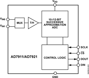
The conversion process and data acquisition are controlled using CS and the serial clock, allowing the devices to interface with microprocessors or DSPs. The input signal is sampled on the falling edge of CS and the conversion is also initiated at this point. There are no pipeline delays associated with the part.
The channel to be converted is selected through the DIN pin and the mode of operation is controlled by CS. The serial data stream from the DOUT pin has a channel identifier bit, which provides information about the channel converted.
The AD7911/AD7921 use advanced design techniques to achieve very low power dissipation at high throughput rates.
The reference for the part is taken internally from VDD. This allows the widest dynamic input range to the ADC. Thus the analog input range for the part is 0 to VDD.
The conversion rate is determined by the SCLK.
At least one model within this product family is in production and available for purchase. The product is appropriate for new designs but newer alternatives may exist.


