
- Manufacturer Part Number : AD9081
- Manufacturer : AD
- Description : MxFE™ Quad, 16-Bit, 12GSPS RFDAC and Quad, 12-Bit, 4GSPS RFADC
- Series : AD9081
- Reference Price : USD 0
- Our Price : We have a better price, contact us by email
- Product Type : Integrated/Special Purpose A/D Converters
- Function : Mixed-Signal Front Ends (MxFE)
- Current Suggest : Pre-Release
- Status : Production
- RoHS Status: -
- Voltage: -
- Feature: -
- Package Case: -
- Temperature Range: -
- Packing: Reel/Tray/Tube
- Standard Packing Quantity: -
- Country of Origin: -
- Other Part Number : AD9081
- Shipping methods : DHL FEDEX UPS TNT
- Delivery Time : Ship within 1 day.
- Manufacturer Production time : 6-8 weeks (Normally have stocks)
- Weight : 0.001KG
Contact us to check the best price and real time inventory quantity for AD9081. If you need any more information about AD9081, you can also send us by email. Our email is [email protected], we will reply you in 12 hours.
- Flexible reconfigurable radio common platform design
- FDD and TDD single and multiband radios
- Tx/Rx channel bandwidth up to 1.6 GHz/2 GHz (4T4R)
- Dual use ADC option (receive and transmit DPD) for TDD
- 4D4A (4 × 3 GSPS to 12 GSPS DAC and 4 × 1.5 GSPS to 4 GSPS ADC)
- Supports transmitter IQ input data rate up to 1.5 Gbps
- Supports receiver IQ output data rate up to 2 Gbps
- RF DAC/RF ADC output/input −3 dB bandwidth of 5.2 GHzand 7.5 GHz
- On-chip PLL (6 GHz to 12 GHz) with multichip synchronization and output clock provided
- External RF clock input option
- AC performance target
- ADC test conditions (3 GSPS, −1 dBFS, fIN < 1.4 GHz)
- NSD = −149 dBFS/Hz, HD2 < −70 dBc, HD3 < −70 dBc, SFDR (excluding HD2, HD3) < −78 dBc; IL < −75 dBc
- DAC test conditions (12 GSPS, −7 dBFS, 2.65 GHz)
- NSD = −158 dBFS/Hz, SFDR < −74 dBc
- ADC test conditions (3 GSPS, −1 dBFS, fIN < 1.4 GHz)
- Versatile Digital Features
- Supports real or complex digital data (8-, 12-, or 16-bit)
- Configurable digital up/down conversion (DDC/DUC)
- 8 fine complex DUCs and 4 coarse complex DUCs
- 8 fine complex DDCs and 4 coarse complex DDCs
- 2 independent NCOs per DUC/DDC
- Option to bypass fine and course DUC/DDC
- Programmable 192-tap FIR filter
- Receiver AGC support
- Fast Detect with low latency for fast AGC control
- Signal Monitor for slow AGC control
- Dedicated AGC support pins
- Transmitter DPD support
- Fine DUC channel gain control and delay adjust
- Coarse DDC delay adjust for ADC observation path
- Auxiliary Features
- Fast frequency hopping
- Low latency digital loopback mode (ADC to DAC)
- ADC clock driver with selectable divide ratios
- Power amplifier downstream protection circuitry
- On-chip temperature sensor
- Programmable GPIO pins
- ADC clock driver with selectable divide ratios
- TDD power savings option
- SERDES JESD204B/C Interface, 16 lanes up to 24.75 Gbps
- 8 receive lanes for RF DAC
- 8 transmit lanes for RF ADC
- JESD204B compatible with the maximum 15.5 Gbps lanerate
- JESD204C compatible with the maximum 24.75 Gbps lanerate
- Sample/bit repeat mode for receive lane rate matching
- Target typical ~6 W to 7 W
- 15 mm × 15 mm BGA with 0.8 mm pitch
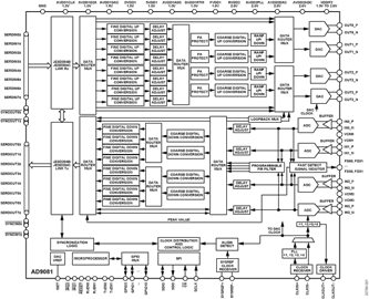
The mixed signal front end (MxFE®) is a high integration device with a 16-bit, 12 GSPS maximum sample rate radio frequency (RF) digital-to-analog converter (DAC) core and a 12-bit, 4 GSPS rate RF analog-to-digital converter (ADC) core. The AD9081 features a 16-lane, 24.75 Gbps JESD204C or 15.5 Gbps JESD204B data transceiver port, an on-chip clock multiplier, and digital signal processing capability targeted at single- and dual-band directto-RF radio applications
The AD9081 supports four transmitter channels and four receiver channels with a 4D4A configuration. The receiver ADC channels can be shared with observation channels in time division duplex (TDD) operating mode. The AD9081 directly addresses the emerging base station applications with high integration and common platform requirements. The device has flexible interpolation/decimation configurations that enable direct-to-RF multiband radio applications. AD9081 supports a complex transmit input data rate up to 6 GSPS and a receive output data rate in single-channel mode up to 4 GSPS. The maximum radio band spacing supported in multichannel modes is 1.2 GHz.
AD9081 features a bypassable interpolator and decimator for achieving ultrawideband capability with low latency loop back and frequency hopping modes targeted at phase array radar system and electronic warfare jammer applications.
Applications
- Wireless communications infrastructure
- W-CDMA, LTE, LTE-A, Massive-MIMO
- Microwave point-to-point and E-Band 5G mmWave
- Broadband communications systems
- DOCSIS 3.0 CMTS
- Phased array radar and electronic warfare
- Electronic test and measurement systems
This product is new and engineering validation may still be underway. Quantities may be limited and design specifications may change while we ready the product for release to production.


