
- Manufacturer Part Number : AD9228
- Manufacturer : AD
- Description : Quad, 12-Bit, 40/65 MSPS Serial LVDS 1.8 V A/D Converter
- Series : AD9228
- Reference Price : USD 16.68
- Our Price : We have a better price, contact us by email
- Product Type : High Speed A/D Converters >10 MSPS
- Function : Standard High Speed A/D Converters >20 MSPS
- Current Suggest : Production
- Status : Production
- RoHS Status: -
- Voltage: -
- Feature: -
- Package Case: -
- Temperature Range: -
- Packing: Reel/Tray/Tube
- Standard Packing Quantity: -
- Country of Origin: -
- Other Part Number : AD9228
- Shipping methods : DHL FEDEX UPS TNT
- Delivery Time : Ship within 1 day.
- Manufacturer Production time : 6-8 weeks (Normally have stocks)
- Weight : 0.001KG
Contact us to check the best price and real time inventory quantity for AD9228. If you need any more information about AD9228, you can also send us by email. Our email is [email protected], we will reply you in 12 hours.
- 4 ADCs integrated into 1 package
- 119 mW ADC power per channel at 65 MSPS
- SNR = 70 dB (to Nyquist)
- ENOB = 11.3 bits
- SFDR = 82 dBc (to Nyquist)
- Excellent linearity
- DNL = ±0.3 LSB (typical)
- INL = ±0.4 LSB (typical)
- Serial LVDS (ANSI-644, default)
Low power, reduced signal option (similar to IEEE 1596.3) - Data and frame clock outputs
- 315 MHz full-power analog bandwidth
- 2 V p-p input voltage range
- 1.8 V supply operation
- Please see the data sheet for additional information
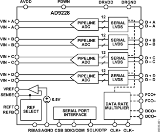
The AD9228 is a quad, 12-bit, 40/65 MSPS analog-to-digital con-verter (ADC) with an on-chip sample-and-hold circuit designedfor low cost, low power, small size, and ease of use. The productoperates at a conversion rate of up to 65 MSPS and is optimized foroutstanding dynamic performance and low power in applications where a small package size is critical.
The ADC requires a single 1.8 V power supply and LVPECL-/ CMOS-/LVDS-compatible sample rate clock for full performanceoperation. No external reference or driver components arerequired for many applications.
The ADC automatically multiplies the sample rate clock for theappropriate LVDS serial data rate. A data clock output (DCO) for capturing data on the output and a frame clock output (FCO) for signaling a new output byte are provided. Individual-channel power-down is supported and typically consumes lessthan 2 mW when all channels are disabled.
The ADC contains several features designed to maximizeflexibility and minimize system cost, such as programmableclock and data alignment and programmable digital test patterngeneration. The available digital test patterns include built-in deterministic and pseudorandom patterns, along with custom user-defined test patterns entered via the serial port interface (SPI).
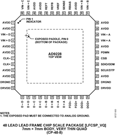
The AD9228 is available in an RoHS compliant, 48-lead LFCSP. It isspecified over the industrial temperature range of −40°C to +85°C.
Product Highlights
- Small Footprint. Four ADCs are contained in a small, space-saving package.
- Low power of 119 mW/channel at 65 MSPS.
- Ease of Use. A data clock output (DCO) is provided that operates at frequencies of up to 390 MHz and supports double data rate (DDR) operation.
- User Flexibility. The SPI control offers a wide range of flexible features to meet specific system requirements.
- Pin-Compatible Family. This includes the AD9287 (8-bit), AD9219 (10-bit), and AD9259 (14-bit).
Applications
- Medical imaging and nondestructive ultrasound
- Portable ultrasound and digital beam-forming systems
- Quadrature radio receivers
- Diversity radio receivers
- Tape drives
- Optical networking
- Test equipment
At least one model within this product family is in production and available for purchase. The product is appropriate for new designs but newer alternatives may exist.


