
- Manufacturer Part Number : AD9229ABCPZ-50
- Manufacturer : AD
- Description : Quad 12-Bit, 50/65 MSPS, Serial LVDS A/D Converter IC
- Series : AD9229
- Reference Price : USD 28.352
- Our Price : We have a better price, contact us by email
- Product Type : High Speed A/D Converters >10 MSPS
- Function : Standard High Speed A/D Converters >20 MSPS
- Current Suggest : Production
- Status : Production
- ROHS Status : ROHS Compliant (Lead Free)
- Package Type : 48-Lead LFCSP (7mm x 7mm x 0.85mm w/ EP)
- Pins : 48
- MFG Package Case : CP-48-8
- Part Type : OTH
- Standard Packing Type : Tray
- Standard Packing Quantity : 260
- Working Temperature : -40 to 85C
- Other Part Number : AD9229ABCPZ-50
- Shipping methods : DHL FEDEX UPS TNT
- Delivery Time : Ship within 1 day.
- Manufacturer Production time : 6-8 weeks (Normally have stocks)
- Weight : 0.001KG
Contact us to check the best price and real time inventory quantity for AD9229ABCPZ-50. If you need any more information about AD9229ABCPZ-50, you can also send us by email. Our email is [email protected], we will reply you in 12 hours.
- Four ADCs in one package
- Small footprint: 7 mm x 7 mm chip scale package
- Serial LVDS digital output data rates up to
- 780 Mbps (ANSI-644)
- Data and Frame clock output provided
- SNR = 69.5 dB (to Nyquist)
- 400 MHz full power analog bandwidth
- Power dissipation = 246 mW per ADC at
50 MSPS - Excellent Linearity:
- DNL = ±0.3 LSB (typical)
- INL = ±0.4 LSB (typical) - 1 V pp – 2 V pp input voltage range
- +3.0 V supply operation
- Power down mode
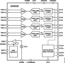
The AD9229 is a 50 or 65 MSPS quad 12-bit, analog–to–digital converter with serial LVDS outputs. An on–chip track–and–hold circuit is designed for low cost, low power, small size and ease of use. The product operates up to a 65 MSPS conversion rate and is optimized for outstanding dynamic performance where a small package size is critical.
The ADC requires a single +3 V power supply. No external reference or driver components are required for many applications. A separate output power supply pin supports LVDS compatible serial digital output levels.
The ADC automatically multiplies up the sample rate clock for the appropriate LVDS serial data rate. This data clock output (DCO) provides operation up to 390 MHz and supports double-data rate operation (DDR). An MSB trigger or Frame clock is also provided to signal a new output byte. Power down is supported, and the ADC consumes 3 mW when enabled.
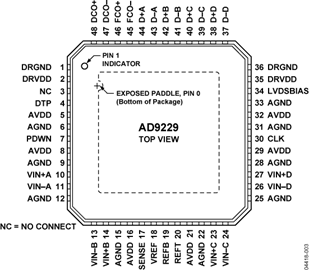
Fabricated on an advanced CMOS process, the AD9229 is available in a 48-pin chip scale 7 mm x 7 mm package (48-LFCSP) specified over the industrial temperature range (–40°C to +85°C).
Applications
At least one model within this product family is in production and available for purchase. The product is appropriate for new designs but newer alternatives may exist.


