
- Manufacturer Part Number : AD9269
- Manufacturer : AD
- Description : 16-Bit, 20 MSPS/40 MSPS/65 MSPS/80 MSPS, 1.8 V Dual Analog-to-Digital Converter
- Series : AD9269
- Reference Price : USD 39.2
- Our Price : We have a better price, contact us by email
- Product Type : High Speed A/D Converters >10 MSPS
- Function : Standard High Speed A/D Converters >20 MSPS
- Current Suggest : Recommended for New Designs
- Status : Production
- RoHS Status: -
- Voltage: -
- Feature: -
- Package Case: -
- Temperature Range: -
- Packing: Reel/Tray/Tube
- Standard Packing Quantity: -
- Country of Origin: -
- Other Part Number : AD9269
- Shipping methods : DHL FEDEX UPS TNT
- Delivery Time : Ship within 1 day.
- Manufacturer Production time : 6-8 weeks (Normally have stocks)
- Weight : 0.001KG
Contact us to check the best price and real time inventory quantity for AD9269. If you need any more information about AD9269, you can also send us by email. Our email is [email protected], we will reply you in 12 hours.
- 1.8 V analog supply operation
- 1.8 V to 3.3 V output supply
- Integrated quadrature error correction (QEC)
- SNR
77.6 dBFS at 9.7 MHz input
71 dBFS at 200 MHz input - SFDR
93 dBc at 9.7 MHz input
80 dBc at 200 MHz input - Low power
44 mW per channel at 20 MSPS
100 mW per channel at 80 MSPS
- Differential input with 700 MHz bandwidth
- On-chip voltage reference and sample-and-hold circuit
- 2V p-p differential analog input
- DNL = −0.5/+1.1 LSB
- Serial port control options
- Offset binary, gray code, or twos complement data format
- Optional clock duty cycle stabilizer (DCS)
- See data sheet for additional features
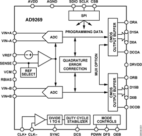
The ADC also contains several features designed to maximize flexibility and minimize system cost, such as programmable clock and data alignment and programmable digital test pattern generation. The available digital test patterns include built-in deterministic and pseudorandom patterns, along with custom user-defined test patterns entered via the serial port interface (SPI).
A differential clock input controls all internal conversion cycles. An optional duty cycle stabilizer (DCS) compensates for wide variations in the clock duty cycle while maintaining excellent overall ADC performance.The digital output data is presented in offset binary, gray code, or twos complement format. A data output clock (DCO) is pro-vided for each ADC channel to ensure proper latch timing with receiving logic. Both 1.8 V and 3.3 V CMOS levels are supported, and output data can be multiplexed onto a single output bus.
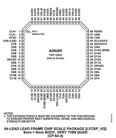
The AD9269 is available in a 64-lead RoHS-compliant LFCSP and is specified over the industrial temperature range (−40°C to +85°C).
Applications- Communications
- Diversity radio systems
- Multimode digital receivers
GSM, EDGE, W-CDMA, LTE, CDMA2000, WiMAX, TD-SCDMA - I/Q demodulation systems
- Smart antenna systems
- Battery-powered instruments
- Hand held scope meters
- Portable medical imaging
- Ultrasound
- Radar/LIDAR
This product has been released to the market. The data sheet contains all final specifications and operating conditions. For new designs, ADI recommends utilization of these products.


