
- Manufacturer Part Number : AD9276BSVZ
- Manufacturer : AD
- Description : Octal LNA/VGA/AAF/12-Bit ADC and CW I/Q Demodulator IC
- Series : AD9276
- Reference Price : USD 46.144
- Our Price : We have a better price, contact us by email
- Product Type : High Speed A/D Converters >10 MSPS
- Function : Standard High Speed A/D Converters >20 MSPS
- Current Suggest : Production
- Status : Production
- ROHS Status : ROHS Compliant (Lead Free)
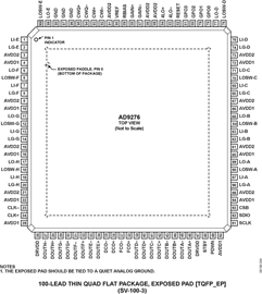
- Package Type : 100-Lead TQFP (14mm x 14mm)
- Pins : 100
- MFG Package Case : SV-100-3
- Part Type : OTH
- Standard Packing Type : Tray
- Standard Packing Quantity : 90
- Working Temperature : -40 to 85C
- Other Part Number : AD9276BSVZ
- Shipping methods : DHL FEDEX UPS TNT
- Delivery Time : Ship within 1 day.
- Manufacturer Production time : 6-8 weeks (Normally have stocks)
- Weight : 0.001KG
Contact us to check the best price and real time inventory quantity for AD9276BSVZ. If you need any more information about AD9276BSVZ, you can also send us by email. Our email is [email protected], we will reply you in 12 hours.
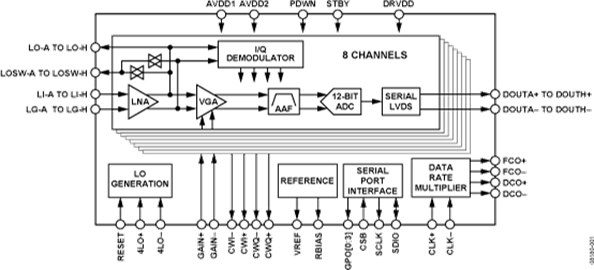
Each channel features a variable gain range of 42 dB, a fully differential signal path, an active input preamplifier termination, a maximum gain of up to 52 dB, and an ADC with a conversion rate of up to 80 MSPS. The channel is optimized for dynamic performance and low power in applications where a small package size is critical.
The LNA has a single-ended-to-differential gain that is selectable through the SPI. The LNA input noise is typically 0.75 nV/√Hz at a gain of 21.3 dB, and the combined input-referred noise of the entire channel is 0.85 nV/√Hz at maximum gain. Assuming a 15 MHz noise bandwidth (NBW) and a 21.3 dB LNA gain, the input SNR is roughly 92 dB. In CW Doppler mode, each LNA output drives an I/Q demodulator. Each demodulator has inde-pendently programmable phase rotation through the SPI with 16 phase settings.
The AD9276 requires a LVPECL-/CMOS-/LVDS-compatible sample rate clock for full performance operation. No external reference or driver components are required for many applications.
The ADC automatically multiplies the sample rate clock for the appropriate LVDS serial data rate. A data clock (DCO±) for capturing data on the output and a frame clock (FCO±) trigger for signaling a new output byte are provided.
Powering down individual channels is supported to increase battery life for portable applications. A standby mode option allows quick power-up for power cycling. In CW Doppler opera-tion, the VGA, AAF, and ADC are powered down. The power of the TGC path scales with selectable ADC speed power modes.
The ADC contains several features designed to maximize flexibility and minimize system cost, such as a programmable clock, data alignment, and programmable digital test pattern generation. The digital test patterns include built-in fixed patterns, built-in pseudo-random patterns, and custom user-defined test patterns entered via the serial port interface.
Fabricated in an advanced CMOS process, the AD9276 is available in a 16 mm × 16 mm, RoHS compliant, 100-lead TQFP. It is specified over the industrial temperature range of −40°C to +85°C.
Product Highlights
- Small Footprint - Eight channels are contained in a small, space-saving package. Full TGC path, ADC, and I/Q demodulator contained within a 100-lead, 16 mm × 16 mm TQFP
- Low Power - In TGC mode, low power of 195 mW per channel at 40 MSPS. In CW mode, ultralow power of 94 mW per channel
- Integrated High Dynamic Range I/Q Demodulator with Phase Rotation
- Ease of Use - A data clock output (DCO±) operates up to 480 MHz and supports double data rate (DDR) operation
- User Flexibility - Serial port interface (SPI) control offers a wide range of flexible features to meet specific system requirements
- Integrated Second-Order Antialiasing Filter - This filter is placed before the ADC and is programmable from 8 MHz to 18 MHz.
- Medical imaging/ultrasound
- Automotive radar
At least one model within this product family is in production and available for purchase. The product is appropriate for new designs but newer alternatives may exist.


