
- Manufacturer Part Number : AD9279BBCZ
- Manufacturer : AD
- Description : Octal LNA/VGA/AAF/ADC and CW I/Q Demodulator IC
- Series : AD9279
- Reference Price : USD 46.4
- Our Price : We have a better price, contact us by email
- Product Type : High Speed A/D Converters >10 MSPS
- Function : Standard High Speed A/D Converters >20 MSPS
- Current Suggest : Recommended for New Designs
- Status : Production
- ROHS Status : ROHS Compliant (Lead Free)
- Package Type : 144-Ball CSPBGA (10mm x 10mm x 1.4mm)
- Pins : 144
- MFG Package Case : BC-144-1
- Part Type : OTH
- Standard Packing Type : Tray
- Standard Packing Quantity : 184
- Working Temperature : -40 to 85C
- Other Part Number : AD9279BBCZ
- Shipping methods : DHL FEDEX UPS TNT
- Delivery Time : Ship within 1 day.
- Manufacturer Production time : 6-8 weeks (Normally have stocks)
- Weight : 0.001KG
Contact us to check the best price and real time inventory quantity for AD9279BBCZ. If you need any more information about AD9279BBCZ, you can also send us by email. Our email is [email protected], we will reply you in 12 hours.
- Lowpower : 141 mW per channel, TGC mode, 40 MSPS;
60 mW per channel, CW mode - 10 mm × 10 mm, 144-ball CSP-BGA
- TGC channel input-referred noise: 0.8 nV/√Hz, max gain
- Flexible power-down modes
- Fast recovery from low power standby mode: <2us
- Overload recovery: <10 ns
- Input-referred noise: 0.75 nV/√Hz , gain = 21.3 dB
- Programmable gain: 15.6 dB/17.9 dB/21.3 dB
- 0.1 dB compression: 1000 mV p-p/750 mV p-p/450 mV p-p
- Dual-mode active input impedance matching
- Bandwidth (BW) > 100 MHz
- Attenuator range: −45 dB to 0 dB
- Postamp gain (PGA): 21 dB/24 dB/27 dB/30 dB
- Linear-in-dB gain control
- Programmable second-order LPF from 8 MHz to 18 MHz
- Programmable HPF
- SNR: 70 dB, 12 bits up to 80 MSPS
- Serial LVDS (ANSI-644, Low power/reduced signal)
- Individual programmable phase rotation
- Output dynamic range per channel: >160 dBc/√Hz
- Output-referred SNR: 155 dBc/√Hz, 1kHz offset, -3dBFS
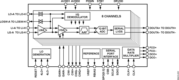
The AD9279 is designed for low cost, low power, small size, and ease of use for medical ultrasound and automotive radar. It contains eight channels of a variable gain amplifier (VGA) with a low noise preamplifier (LNA), an antialiasing filter (AAF), an analog-to-digital converter (ADC), and an I/Q demodulator with programmable phase rotation.
Each channel features a variable gain range of 45 dB, a fully differential signal path, an active input preamplifier termination, and a maximum gain of up to 52 dB. The channel is optimized for high dynamic performance and low power in applications where a small package size is critical.
The LNA has a single-ended-to-differential gain that is selectable through the SPI. Assuming a 15 MHz noise bandwidth (NBW) and a 21.3 dB LNA gain, the LNA input SNR is roughly 94 dB. In CW Doppler mode, each LNA output drives an I/Q demod-ulator that has independently programmable phase rotation with 16 phase settings.
Power-down of individual channels is supported to increase battery life for portable applications. Standby mode allows quick power-up for power cycling. In CW Doppler operation, the VGA, AAF, and ADC are powered down. The ADC contains several features designed to maximize flexibility and minimize system cost, such as a programmable clock, data alignment, and programmable digital test pattern generation. The digital test patterns include built-in fixed patterns, built-in pseudo random patterns, and custom user-defined test patterns entered via the serial port interface.
This product has been released to the market. The data sheet contains all final specifications and operating conditions. For new designs, ADI recommends utilization of these products.


