
- Manufacturer Part Number : AD9430BSVZ-170
- Manufacturer : AD
- Description : 12-Bit, 170/210 MSPS 3.3 V A/D Converter IC
- Series : AD9430
- Reference Price : USD 32.936
- Our Price : We have a better price, contact us by email
- Product Type : High Speed A/D Converters >10 MSPS
- Function : Standard High Speed A/D Converters >20 MSPS
- Current Suggest : Production
- Status : Production
- ROHS Status : ROHS Compliant (Lead Free)
- Package Type : 100-Lead TQFP (14mm x 14mm w/ EP)
- Pins : 100
- MFG Package Case : SV-100-1
- Part Type : OTH
- Standard Packing Type : Tray
- Standard Packing Quantity : 90
- Working Temperature : -40 to 85C
- Other Part Number : AD9430BSVZ-170
- Shipping methods : DHL FEDEX UPS TNT
- Delivery Time : Ship within 1 day.
- Manufacturer Production time : 6-8 weeks (Normally have stocks)
- Weight : 0.001KG
Contact us to check the best price and real time inventory quantity for AD9430BSVZ-170. If you need any more information about AD9430BSVZ-170, you can also send us by email. Our email is [email protected], we will reply you in 12 hours.
- SNR = 65 dB @ Fin up to 70 MHz @
210 MSPS - ENOB of 10.6 @ Fin up to 70 MHz @
210 MSPS - SFDR = 80 dBc @ Fin up to 70 MHz @
210 MSPS - Excellent Linearity:
DNL = ±0.3 LSB (Typical)
INL = ±0.5 LSB (Typical) - Two Output Data Options:
Demultiplexed 3.3 V CMOS Outputs Each @ 105 MSPS
Interleaved or Parallel Data Output Option
LVDS at 210 MSPS
- 700 MHz Full Power Analog Bandwidth
- Power Dissipation = 1.3 W Typical @ 210 MSPS
- 1.5 V Input Voltage Range
- 3.3 V Supply Operation
- Output Data Format Option
- Data Sync Input and Data Clock Output Provided
- Clock Duty Cycle Stabilizer
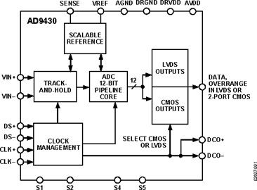
The ADC requires a 3.3 V power supply and a differential ENCODE clock for full performance operation. The digital outputs are TTL/CMOS or LVDS compatible and support either twos complement or offset binary format. Separate output power supply pins support interfacing with 3.3 V or 2.5 V CMOS logic.
Two output buses support demultiplexed data up to 105 MSPS rates in CMOS mode. A data sync input is supported for proper output data port alignment in CMOS mode and a data clock output is available for proper output data timing. In LVDS mode, the chip provides data at the ENCODE clock rate.
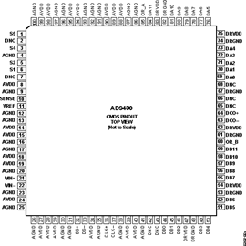
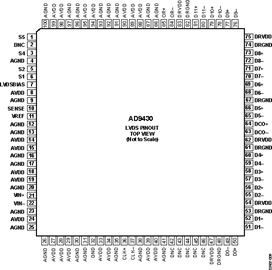
Fabricated on an advanced BiCMOS process, the AD9430 is available in a 100-lead surface-mount plastic package (100 e-PAD TQFP) specified over the industrial temperature range (-40°C to +85°C).
Applications
- Wireless and Wired Broadband Communications
- Cable Reverse Path
- Communications Test Equipment
- Radar and Satellite Subsystems
- Power Amplifier Linearization
At least one model within this product family is in production and available for purchase. The product is appropriate for new designs but newer alternatives may exist.


