
- Manufacturer Part Number : AD9467BCPZ-200
- Manufacturer : AD
- Description : 16-Bit, 200 MSPS/250 MSPS Analog-to-Digital Converter IC
- Series : AD9467
- Reference Price : USD 80.24
- Our Price : We have a better price, contact us by email
- Product Type : High Speed A/D Converters >10 MSPS
- Function : Standard High Speed A/D Converters >20 MSPS
- Current Suggest : Recommended for New Designs
- Status : Production
- ROHS Status : ROHS Compliant (Lead Free)
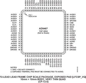
- Package Type : 72-Lead LFCSP (10mm x 10mm w/ EP)
- Pins : 72
- MFG Package Case : CP-72-5
- Part Type : OTH
- Standard Packing Type : Tray
- Standard Packing Quantity : 168
- Working Temperature : -40 to 85C
- Other Part Number : AD9467BCPZ-200
- Shipping methods : DHL FEDEX UPS TNT
- Delivery Time : Ship within 1 day.
- Manufacturer Production time : 6-8 weeks (Normally have stocks)
- Weight : 0.001KG
Contact us to check the best price and real time inventory quantity for AD9467BCPZ-200. If you need any more information about AD9467BCPZ-200, you can also send us by email. Our email is [email protected], we will reply you in 12 hours.
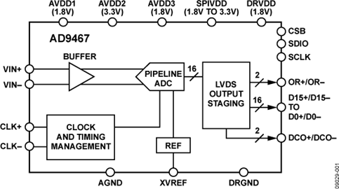
The ADC requires 1.8 V and 3.3 V power supplies and a low voltage differential input clock for full performance operation. No external reference or driver components are required for many applications. Data outputs are LVDS compatible (ANSI-644 compatible) and include the means to reduce the overall current needed for short trace distances.
A data clock output (DCO) for capturing data on the output is provided for signaling a new output bit.
The internal power-down feature supported via the SPI and typically consumes less than 5 mW when disabled.
Optional features allow users to implement various selectable operating conditions, including input range, data format select, and output data test patterns.
The AD9467 is available in a Pb-free, 72-lead, LFCSP specified over the −40°C to +85°C industrial temperature range.
Product Highlights
- IF optimization capability used to improve SFDR.
- Outstanding SFDR performance for IF sampling applications such as multicarrier, multimode 3G, and 4G cellular base station receivers.
- Ease of use: on-chip reference, high input impedance buffer, adjustable analog input range, and an output clock to simplify data capture.
- Packaged in a Pb-free, 72-lead LFCSP package.
- Clock duty cycle stabilizer (DCS) maintains overall ADC performance over a wide range of input clock pulse widths.
- Standard serial port interface (SPI) supports various product features and functions, such as data formatting (offset binary, twos complement, or Gray coding), enabling the clock DCS.
Applications
- Multicarrier, multimode cellular receivers
- Antenna array positioning
- Power amplifier linearization
- Broadband wireless
- Radar
- Infrared imaging
- Communications instrumentation
This product has been released to the market. The data sheet contains all final specifications and operating conditions. For new designs, ADI recommends utilization of these products.


