
- Manufacturer Part Number : AD9467
- Manufacturer : AD
- Description : 16-Bit, 200 MSPS/250 MSPS Analog-to-Digital Converter
- Series : AD9467
- Reference Price : USD 80.24
- Our Price : We have a better price, contact us by email
- Product Type : High Speed A/D Converters >10 MSPS
- Function : Standard High Speed A/D Converters >20 MSPS
- Current Suggest : Recommended for New Designs
- Status : Production
- RoHS Status: -
- Voltage: -
- Feature: -
- Package Case: -
- Temperature Range: -
- Packing: Reel/Tray/Tube
- Standard Packing Quantity: -
- Country of Origin: -
- Other Part Number : AD9467
- Shipping methods : DHL FEDEX UPS TNT
- Delivery Time : Ship within 1 day.
- Manufacturer Production time : 6-8 weeks (Normally have stocks)
- Weight : 0.001KG
Contact us to check the best price and real time inventory quantity for AD9467. If you need any more information about AD9467, you can also send us by email. Our email is [email protected], we will reply you in 12 hours.
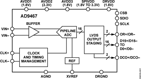
The ADC requires 1.8 V and 3.3 V power supplies and a low voltage differential input clock for full performance operation. No external reference or driver components are required for many applications. Data outputs are LVDS compatible (ANSI-644 compatible) and include the means to reduce the overall current needed for short trace distances.
A data clock output (DCO) for capturing data on the output is provided for signaling a new output bit.
The internal power-down feature supported via the SPI and typically consumes less than 5 mW when disabled.
Optional features allow users to implement various selectable operating conditions, including input range, data format select, and output data test patterns.
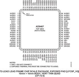
The AD9467 is available in a Pb-free, 72-lead, LFCSP specified over the −40°C to +85°C industrial temperature range.
Product Highlights
- IF optimization capability used to improve SFDR.
- Outstanding SFDR performance for IF sampling applications such as multicarrier, multimode 3G, and 4G cellular base station receivers.
- Ease of use: on-chip reference, high input impedance buffer, adjustable analog input range, and an output clock to simplify data capture.
- Packaged in a Pb-free, 72-lead LFCSP package.
- Clock duty cycle stabilizer (DCS) maintains overall ADC performance over a wide range of input clock pulse widths.
- Standard serial port interface (SPI) supports various product features and functions, such as data formatting (offset binary, twos complement, or Gray coding), enabling the clock DCS.
Applications
- Multicarrier, multimode cellular receivers
- Antenna array positioning
- Power amplifier linearization
- Broadband wireless
- Radar
- Infrared imaging
- Communications instrumentation
This product has been released to the market. The data sheet contains all final specifications and operating conditions. For new designs, ADI recommends utilization of these products.


