
- Manufacturer Part Number : AD9508/PCBZ
- Manufacturer : AD
- Description : 8-Bit, 500 MSPS, 1.8 V Analog-to-Digital Converter IC
- Series : AD9484
- Reference Price : USD 0
- Our Price : We have a better price, contact us by email
- Product Type : High Speed A/D Converters >10 MSPS
- Function : Standard High Speed A/D Converters >20 MSPS
- Current Suggest : Recommended for New Designs
- Status : Production
- ROHS Status : ROHS Compliant (Lead Free)
- Package Type : Evaluation Board
- Pins : -
- MFG Package Case : -
- Part Type : EVAL
- Standard Packing Type : -
- Standard Packing Quantity : -
- Working Temperature : -
- Other Part Number : AD9508/PCBZ
- Shipping methods : DHL FEDEX UPS TNT
- Delivery Time : Ship within 1 day.
- Manufacturer Production time : 6-8 weeks (Normally have stocks)
- Weight : 0.001KG
Contact us to check the best price and real time inventory quantity for AD9508/PCBZ. If you need any more information about AD9508/PCBZ, you can also send us by email. Our email is [email protected], we will reply you in 12 hours.
- SNR = 47 dBFS at fIN up to
250 MHz at 500 MSPS - ENOB of 7.5 bits at fIN up to
250 MHz at 500 MSPS
(−1.0 dBFS) - SFDR = 79 dBc at fIN up to
250 MHz at 500 MSPS
(−1.0 dBFS) - Integrated input buffer
- Excellent linearity
-- DNL = ±0.1 LSB typical
-- INL = ±0.1 LSB typical - LVDS at 500 MSPS
(ANSI-644 levels) - 1 GHz full power analog bandwidth
- Pin Compatible with AD9434 and AD9230, ADCs
- See datasheet for additional features
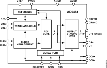
The AD9484 is an 8-bit, monolithic, sampling analog-to-digital converter (ADC) optimized for high performance, low power, and ease of use. The part operates at up to a 500 MSPS conversion rate and is optimized for outstanding dynamic performance in wideband carrier and broadband systems. All necessary functions, including a sample-and-hold and voltage reference, are included on the chip to provide a complete signal conversion solution. The VREF pin can be used to monitor the internal reference or provide an external voltage reference (external reference mode must be enabled through the SPI port).
The ADC requires a 1.8 V analog voltage supply and a differential clock for full performance operation. The digital outputs are LVDS (ANSI-644) compatible and support twos complement, offset binary format, or Gray code. A data clock output is available for proper output data timing.
Fabricated on an advanced BiCMOS process, the AD9484 is available in a 56-lead LFCSP, and is specified over the industrial temperature range (−40°C to +85°C). This product is protected under U.S. and international patents.
APPLICATIONS
- Wireless and wired broadband communications
- Cable reverse path
- Communications test equipment
- Low cost digital oscilloscopes
- Satellite subsystems
- Power amplifier linearization
- High Performance.
Maintains 47 dBFS SNR at 500 MSPS with a 250 MHz input. - Ease of Use.
LVDS output data and output clock signal allow interface to current FPGA technology. The on-chip reference and sample and hold provide flexibility in system design. Use of a single 1.8 V supply simplifies system power supply design. - Serial Port Control.
Standard serial port interface supports various product functions, such as data formatting, disabling the clock duty cycle stabilizer, power-down, gain adjust, and output test pattern generation. - Pin compatible with AD9434, 12-bit 500Msps and AD9230, 12-bit 250Msps ADCs.
This product has been released to the market. The data sheet contains all final specifications and operating conditions. For new designs, ADI recommends utilization of these products.


