
- Manufacturer Part Number : AD9626
- Manufacturer : AD
- Description : 12-Bit, 170 MSPS/210 MSPS/250 MSPS, 1.8 V Analog-to-Digital Converter
- Series : AD9626
- Reference Price : USD 28.768
- Our Price : We have a better price, contact us by email
- Product Type : High Speed A/D Converters >10 MSPS
- Function : Standard High Speed A/D Converters >20 MSPS
- Current Suggest : Production
- Status : Production
- RoHS Status: -
- Voltage: -
- Feature: -
- Package Case: -
- Temperature Range: -
- Packing: Reel/Tray/Tube
- Standard Packing Quantity: -
- Country of Origin: -
- Other Part Number : AD9626
- Shipping methods : DHL FEDEX UPS TNT
- Delivery Time : Ship within 1 day.
- Manufacturer Production time : 6-8 weeks (Normally have stocks)
- Weight : 0.001KG
Contact us to check the best price and real time inventory quantity for AD9626. If you need any more information about AD9626, you can also send us by email. Our email is [email protected], we will reply you in 12 hours.
- SNR = 64.8 dBFS @ fIN up to 70 MHz @
250 MSPS - ENOB of 10.5 @ fIN up to 70 MHz @
250 MSPS (−1.0 dBFS) - SFDR = 80 dBc @ fIN up to 70 MHz @
250 MSPS (−1.0 dBFS) - Excellent Linearity
DNL = ±0.3 LSB typical
INL = ±0.7 LSB typical - CMOS outputs
Single data port at up to 250 MHz
Interleaved dual port @ 1/2 sample rate up to 125 MHz - 700 MHz full power analog bandwidth
- On-chip reference, no external decoupling required
- Integrated input buffer and track-and-hold
- Low power dissipation
272 mW @ 170 MSPS
364 mW @ 250 MSPS - Programmable input voltage range
1.0 V to 1.5 V, 1.25 V nominal - 1.8 V analog and digital supply operation
- Selectable output data format (offset binary, twos complement, Gray code)
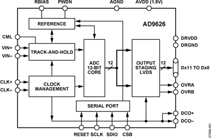
The ADC requires a 1.8 V analog voltage supply and a differential clock for full performance operation. The digital outputs are CMOS compatible and support either twos complement, offset binary format, or Gray code. A data clock output is available for proper output data timing.
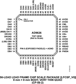
Fabricated on an advanced CMOS process, the AD9626 is available in a 56-lead LFCSP, specified over the industrial temperature range (−40°C to +85°C).
Product Highlights
- High Performance–Maintains 64.9 dBFS SNR @ 250 MSPS with a 70 MHz input.
- Low Power–Consumes only 364 mW @ 250 MSPS.
- Ease of Use–CMOS output data and output clock signal allow interface to current FPGA technology. The on-chip reference and sample-and-hold provide flexibility in system design. Use of a single 1.8 V supply simplifies system power supply design.
- Serial Port Control–Standard serial port interface supports various product functions, such as data formatting, clock duty cycle stabilizer, power-down, gain adjust, and output test pattern generation.
- Pin-Compatible Family–10-bit pin-compatible family offered as the AD9601.
Applications
- Wireless and wired broadband communications
- Cable reverse path
- Communications test equipment
- Radar and satellite subsystems
- Power amplifier linearization
At least one model within this product family is in production and available for purchase. The product is appropriate for new designs but newer alternatives may exist.


