
- Manufacturer Part Number : AD9627-150EBZ
- Manufacturer : AD
- Description : 12-Bit, 170 MSPS/210 MSPS/250 MSPS, 1.8 V Analog-to-Digital Converter IC
- Series : AD9626
- Reference Price : USD 0
- Our Price : We have a better price, contact us by email
- Product Type : High Speed A/D Converters >10 MSPS
- Function : Standard High Speed A/D Converters >20 MSPS
- Current Suggest : Production
- Status : Production
- ROHS Status : ROHS Compliant (Lead Free)
- Package Type : Evaluation Board
- Pins : -
- MFG Package Case : -
- Part Type : EVAL
- Standard Packing Type : -
- Standard Packing Quantity : -
- Working Temperature : -
- Other Part Number : AD9627-150EBZ
- Shipping methods : DHL FEDEX UPS TNT
- Delivery Time : Ship within 1 day.
- Manufacturer Production time : 6-8 weeks (Normally have stocks)
- Weight : 0.001KG
Contact us to check the best price and real time inventory quantity for AD9627-150EBZ. If you need any more information about AD9627-150EBZ, you can also send us by email. Our email is [email protected], we will reply you in 12 hours.
- SNR = 64.8 dBFS @ fIN up to 70 MHz @
250 MSPS - ENOB of 10.5 @ fIN up to 70 MHz @
250 MSPS (−1.0 dBFS) - SFDR = 80 dBc @ fIN up to 70 MHz @
250 MSPS (−1.0 dBFS) - Excellent Linearity
DNL = ±0.3 LSB typical
INL = ±0.7 LSB typical - CMOS outputs
Single data port at up to 250 MHz
Interleaved dual port @ 1/2 sample rate up to 125 MHz - 700 MHz full power analog bandwidth
- On-chip reference, no external decoupling required
- Integrated input buffer and track-and-hold
- Low power dissipation
272 mW @ 170 MSPS
364 mW @ 250 MSPS - Programmable input voltage range
1.0 V to 1.5 V, 1.25 V nominal - 1.8 V analog and digital supply operation
- Selectable output data format (offset binary, twos complement, Gray code)
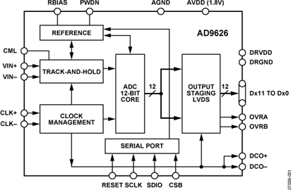
The ADC requires a 1.8 V analog voltage supply and a differential clock for full performance operation. The digital outputs are CMOS compatible and support either twos complement, offset binary format, or Gray code. A data clock output is available for proper output data timing.
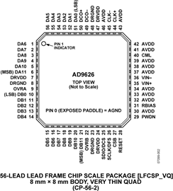
Fabricated on an advanced CMOS process, the AD9626 is available in a 56-lead LFCSP, specified over the industrial temperature range (−40°C to +85°C).
Product Highlights
- High Performance–Maintains 64.9 dBFS SNR @ 250 MSPS with a 70 MHz input.
- Low Power–Consumes only 364 mW @ 250 MSPS.
- Ease of Use–CMOS output data and output clock signal allow interface to current FPGA technology. The on-chip reference and sample-and-hold provide flexibility in system design. Use of a single 1.8 V supply simplifies system power supply design.
- Serial Port Control–Standard serial port interface supports various product functions, such as data formatting, clock duty cycle stabilizer, power-down, gain adjust, and output test pattern generation.
- Pin-Compatible Family–10-bit pin-compatible family offered as the AD9601.
Applications
- Wireless and wired broadband communications
- Cable reverse path
- Communications test equipment
- Radar and satellite subsystems
- Power amplifier linearization
At least one model within this product family is in production and available for purchase. The product is appropriate for new designs but newer alternatives may exist.


