Email: [email protected]
Hot Selling IC

Enter a Part Number:

Best Price NOW
Manufacturer / Brand: AD
Details: 12-Bit, 20 MSPS/40 MSPS/65 MSPS/80 MSPS, 1.8 V Analog-to-Digital Converter
Series: AD9629
Quantity Available: Over 47460 pieces
Our Email: [email protected]
Product Parameters
- Manufacturer Part Number : AD9629
- Manufacturer : AD
- Description : 12-Bit, 20 MSPS/40 MSPS/65 MSPS/80 MSPS, 1.8 V Analog-to-Digital Converter
- Series : AD9629
- Reference Price : USD 4.328
- Our Price : We have a better price, contact us by email
- Product Type : High Speed A/D Converters >10 MSPS
- Function : Standard High Speed A/D Converters >20 MSPS
- Current Suggest : Production
- Status : Production
- RoHS Status: -
- Voltage: -
- Feature: -
- Package Case: -
- Temperature Range: -
- Packing: Reel/Tray/Tube
- Standard Packing Quantity: -
- Country of Origin: -
- Other Part Number : AD9629
- Shipping methods : DHL FEDEX UPS TNT
- Delivery Time : Ship within 1 day.
- Manufacturer Production time : 6-8 weeks (Normally have stocks)
- Weight : 0.001KG
Contact us to check the best price and real time inventory quantity for AD9629. If you need any more information about AD9629, you can also send us by email. Our email is [email protected], we will reply you in 12 hours.
Request Quotation for AD9629
Related IC Components
Features and Benefits of AD9629
Product Detailed Description for AD9629
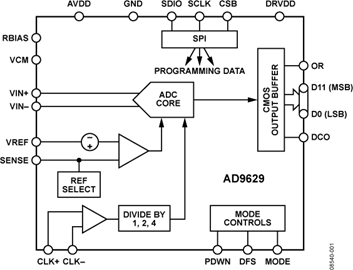
The AD9629 is a monolithic, single channel 1.8 V supply, 12-bit, 20 MSPS/40 MSPS/65MSPS/80 MSPS analog-to-digital converter (ADC). It features a high performance sample-and-hold circuit and on-chip voltage reference.
The product uses multistage differential pipeline architecture with output error correction logic to provide 12-bit accuracy at 80 MSPS data rates and to guarantee no missing codes over the full operating temperature range.
The ADC contains several features designed to maximize flexibility and minimize system cost, such as programmable clock and data alignment and programmable digital test pattern generation. The available digital test patterns include built-in deterministic and pseudorandom patterns, along with custom user-defined test patterns entered via the serial port interface (SPI).
A differential clock input with optional 1, 2, or 4 divide ratios controls all internal conversion cycles.
The digital output data is presented in offset binary, gray code, or twos complement format. A data output clock (DCO) is provided to ensure proper latch timing with receiving logic. Both 1.8 V and 3.3 V CMOS levels are supported.
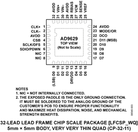
The AD9629 is available in a 32-lead RoHS compliant LFCSP and is specified over the industrial temperature range (−40°C to +85°C).
Product Highlights
1. The AD9629 operates from a single 1.8 V analog power supply and features a separate digital output driver supply to accommodate 1.8 V to 3.3 V logic families.
2. The sample-and-hold circuit maintains excellent performance for input frequencies up to 200 MHz and is designed for low cost, low power, and ease of use.
3. A standard serial port interface (SPI) supports various product features and functions, such as data output formatting, internal clock divider, power-down, DCO and data output (D11 to D0) timing and offset adjustments, and voltage reference modes.
4. The AD9629 is packaged in a 32-lead RoHS compliant LFCSP that is pin compatible with the AD9609 10-bit ADC and the AD9649 14-bit ADC, enabling a simple migration path between 10-bit and 14-bit converters sampling from 20 MSPS to 80 MSPS.
The product uses multistage differential pipeline architecture with output error correction logic to provide 12-bit accuracy at 80 MSPS data rates and to guarantee no missing codes over the full operating temperature range.
The ADC contains several features designed to maximize flexibility and minimize system cost, such as programmable clock and data alignment and programmable digital test pattern generation. The available digital test patterns include built-in deterministic and pseudorandom patterns, along with custom user-defined test patterns entered via the serial port interface (SPI).
A differential clock input with optional 1, 2, or 4 divide ratios controls all internal conversion cycles.
The digital output data is presented in offset binary, gray code, or twos complement format. A data output clock (DCO) is provided to ensure proper latch timing with receiving logic. Both 1.8 V and 3.3 V CMOS levels are supported.
The AD9629 is available in a 32-lead RoHS compliant LFCSP and is specified over the industrial temperature range (−40°C to +85°C).
Applications
- Communications
- Diversity radio systems
- Multimode digital receivers
- GSM, EDGE, W-CDMA, LTE, CDMA2000, WiMAX, TD-SCDMA
- Smart antenna systems
- Battery-powered instruments
- Hand held scope meters
- Portable medical imaging
- Ultrasound
- Radar/LIDAR
- PET/SPECT imaging
Product Highlights
1. The AD9629 operates from a single 1.8 V analog power supply and features a separate digital output driver supply to accommodate 1.8 V to 3.3 V logic families.
2. The sample-and-hold circuit maintains excellent performance for input frequencies up to 200 MHz and is designed for low cost, low power, and ease of use.
3. A standard serial port interface (SPI) supports various product features and functions, such as data output formatting, internal clock divider, power-down, DCO and data output (D11 to D0) timing and offset adjustments, and voltage reference modes.
4. The AD9629 is packaged in a 32-lead RoHS compliant LFCSP that is pin compatible with the AD9609 10-bit ADC and the AD9649 14-bit ADC, enabling a simple migration path between 10-bit and 14-bit converters sampling from 20 MSPS to 80 MSPS.
Lifecycle information of AD9629
At least one model within this product family is in production and available for purchase. The product is appropriate for new designs but newer alternatives may exist.
AD9629 More photos


Email: [email protected]
Stocking Distributor for All series AD IC
Copyright © 2001-2020 BYCHIPS Limited

