
- Manufacturer Part Number : AD9641BCPZRL7-80
- Manufacturer : AD
- Description : 14-Bit, 80 MSPS/155 MSPS, 1.8 V Serial Output Analog-to-Digital Converter (ADC) IC
- Series : AD9641
- Reference Price : USD 21.08
- Our Price : We have a better price, contact us by email
- Product Type : High Speed A/D Converters >10 MSPS
- Function : Standard High Speed A/D Converters >20 MSPS
- Current Suggest : Recommended for New Designs
- Status : Production
- ROHS Status : ROHS Compliant (Lead Free)
- Package Type : 32-Lead LFCSP (5mm x 5mm x 0.75mm w/ EP)
- Pins : 32
- MFG Package Case : CP-32-12
- Part Type : REEL
- Standard Packing Type : Reel
- Standard Packing Quantity : 1500
- Working Temperature : -40 to 85C
- Other Part Number : AD9641BCPZRL7-80
- Shipping methods : DHL FEDEX UPS TNT
- Delivery Time : Ship within 1 day.
- Manufacturer Production time : 6-8 weeks (Normally have stocks)
- Weight : 0.001KG
Contact us to check the best price and real time inventory quantity for AD9641BCPZRL7-80. If you need any more information about AD9641BCPZRL7-80, you can also send us by email. Our email is [email protected], we will reply you in 12 hours.
- JESD204A coded serial digital outputs
- SNR = 73.7 dBFS @70 MHz and 80MSPS
- SNR = 72.8 dBFS @70 MHz and 155MSPS
- SFDR = 94 dBc @ 70 MHz and 80 MSPS
- SFDR = 90 dBc @ 70 MHz and 155 MSPS Low power: 238 mW @ 80 MSPS 1.8 V supply operation
- Low power: 238 mW @ 80 MSPS, 313mW at 155 MSPS
- 1.8 V supply operation
- Integer 1-to-8 input clock divider
- IF sampling frequencies to 250 MHz
- Please see data sheet for additional features
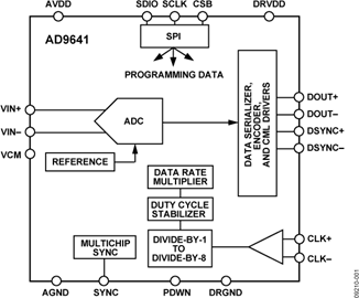
The ADC core features a multistage, differential pipelined architecture with integrated output error correction logic. The ADC features wide bandwidth, differential sample-and-hold, analog input amplifiers that support a variety of user-selectable input ranges. An integrated voltage reference eases the design considerations. A duty cycle stabilizer (DCS) is provided to compensate for variations in the ADC clock duty cycle, allowing the converter to maintain excellent performance.
The ADC output data is routed directly to the JESD204A serial output port. This output is at CML voltage levels. A CMOS or LVDS synchronization input (DSYNC) is provided.
The flexible power-down options allow significant power savings, when desired.
Programming for setup and control is accomplished using a 3-wire SPI-compatible serial interface.
The AD9641 is available in a 32-lead LFCSP and is specified over the industrial temperature range of −40°C to +85°C.
Applications
- Communications
- Diversity radio systems
- Multimode digital receivers (3G and 4G)
GSM, EDGE, W-CDMA, LTE,
CDMA2000, WiMAX, TD-SCDMA - Smart antenna systems
- General-purpose software radios
- Broadband data applications
- Ultrasound equipment
Product Highlights
- An on-chip PLL allows users to provide a single ADC sampling clock. The PLL multiplies the ADC sampling clock to produce the corresponding JESD204A data rate clock.
- The configurable JESD204A output block coded data rate supports up to 1.6 Gbps.
- A proprietary differential input maintains excellent SNR performance for input frequencies up to 250 MHz.
- Operation is from a single 1.8 V power supply.
- The standard serial port interface (SPI) supports various product features and functions, such as data formatting (offset binary, twos complement, or gray coding), controlling the clock DCS, power-down, test modes, voltage reference mode, and serial output configuration.
This product has been released to the market. The data sheet contains all final specifications and operating conditions. For new designs, ADI recommends utilization of these products.


