
- Manufacturer Part Number : AD9652BBCZ-310
- Manufacturer : AD
- Description : 16-bit, 310 MSPS, 3.3/1.8 V Dual Analog-to-Digital Converter (ADC) IC
- Series : AD9652
- Reference Price : USD 185
- Our Price : We have a better price, contact us by email
- Product Type : High Speed A/D Converters >10 MSPS
- Function : Standard High Speed A/D Converters >20 MSPS
- Current Suggest : Recommended for New Designs
- Status : Production
- ROHS Status : ROHS Compliant (Lead Free)
- Package Type : 144-Ball CSPBGA (10mm x 10mm)
- Pins : 144
- MFG Package Case : BC-144-6
- Part Type : OTH
- Standard Packing Type : Tray
- Standard Packing Quantity : 184
- Working Temperature : -40 to 85C
- Other Part Number : AD9652BBCZ-310
- Shipping methods : DHL FEDEX UPS TNT
- Delivery Time : Ship within 1 day.
- Manufacturer Production time : 6-8 weeks (Normally have stocks)
- Weight : 0.001KG
Contact us to check the best price and real time inventory quantity for AD9652BBCZ-310. If you need any more information about AD9652BBCZ-310, you can also send us by email. Our email is [email protected], we will reply you in 12 hours.
- High Dynamic Range
- SNR = 75.0 dBFS at 70 MHz
(AIN = −1 dBFS)
- SFDR = 87 dBc at 70 MHz
(AIN = −1 dBFS)
- See data sheet for additional features - Excellent IF Sampling Performance
- SNR = 73.7 dBFS at 170 MHz (AIN = −1 dBFS)
- SFDR = 85 dBc at 170 MHz
(AIN = −1 dBFS)
- Full power bandwidth of 465 MHz - On-chip 3.3 V buffer
- Programmable input span of 2 V p-p to 2.5 V p-p (default)
- Differential clock input receiver with 1, 2, 4, and 8 integer inputs (clock divider input accepts up to 1.24 GHz)
- Internal ADC clock duty cycle stabilizer
- SYNC input allows multichip synchronization
- Total power consumption:
2.16 W
- 3.3 V and 1.8 V supply voltages - DDR LVDS (ANSI-644 levels) outputs
- Serial port control
- Energy saving power-down modes
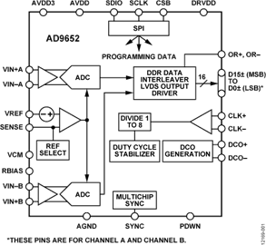
The dual ADC cores feature a multistage, pipelined architecture with integrated output error correction logic. A high performance on-chip buffer and internal voltage reference simplify the inter-face to external driving circuitry while preserving the exceptional performance of the ADC.
The AD9652 can support input clock frequencies of up to 1.24 GHz with a 1, 2, 4, and 8 integer clock divider used to generate the ADC sample clock. A duty cycle stabilizer is provided to compensate for variations in the ADC clock duty cycle. The 16-bit output data (with an overrange bit) from each ADC is interleaved onto a single LVDS output port along with a double data rate (DDR) clock. Programming for setup and control are accomplished using a 3-wire SPI-compatible serial interface.
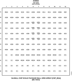
The AD9652 is available in a 144-ball CSP_BGA and is specified over the industrial temperature range of −40°C to +85°C. This product is protected by pending U.S. patents.
PRODUCT HIGHLIGHTS
- Integrated dual, 16-bit, 310 MSPS ADCs.
- On-chip buffer simplifies ADC driver interface.
- Operation from a 3.3 V and 1.8 V supply and a separate digital
output driver supply accommodating LVDS outputs. - Proprietary differential input maintains excellent SNR
performance for input frequencies of up to 485 MHz. - SYNC input allows synchronization of multiple devices.
- Three-wire, 3.3 V or 1.8 V SPI port for register programming
and readback.
APPLICATIONS
- Miltary radar and communications
- Multimode digital receivers (3G or 4G)
- Test and Instrumentation
- Smart antenna systems
This product has been released to the market. The data sheet contains all final specifications and operating conditions. For new designs, ADI recommends utilization of these products.


