
- Manufacturer Part Number : AD9652
- Manufacturer : AD
- Description : 16-bit, 310 MSPS, 3.3/1.8 V Dual Analog-to-Digital Converter (ADC)
- Series : AD9652
- Reference Price : USD 185
- Our Price : We have a better price, contact us by email
- Product Type : High Speed A/D Converters >10 MSPS
- Function : Standard High Speed A/D Converters >20 MSPS
- Current Suggest : Recommended for New Designs
- Status : Production
- RoHS Status: -
- Voltage: -
- Feature: -
- Package Case: -
- Temperature Range: -
- Packing: Reel/Tray/Tube
- Standard Packing Quantity: -
- Country of Origin: -
- Other Part Number : AD9652
- Shipping methods : DHL FEDEX UPS TNT
- Delivery Time : Ship within 1 day.
- Manufacturer Production time : 6-8 weeks (Normally have stocks)
- Weight : 0.001KG
Contact us to check the best price and real time inventory quantity for AD9652. If you need any more information about AD9652, you can also send us by email. Our email is [email protected], we will reply you in 12 hours.
- High Dynamic Range
- SNR = 75.0 dBFS at 70 MHz
(AIN = −1 dBFS)
- SFDR = 87 dBc at 70 MHz
(AIN = −1 dBFS)
- See data sheet for additional features - Excellent IF Sampling Performance
- SNR = 73.7 dBFS at 170 MHz (AIN = −1 dBFS)
- SFDR = 85 dBc at 170 MHz
(AIN = −1 dBFS)
- Full power bandwidth of 465 MHz - On-chip 3.3 V buffer
- Programmable input span of 2 V p-p to 2.5 V p-p (default)
- Differential clock input receiver with 1, 2, 4, and 8 integer inputs (clock divider input accepts up to 1.24 GHz)
- Internal ADC clock duty cycle stabilizer
- SYNC input allows multichip synchronization
- Total power consumption:
2.16 W
- 3.3 V and 1.8 V supply voltages - DDR LVDS (ANSI-644 levels) outputs
- Serial port control
- Energy saving power-down modes
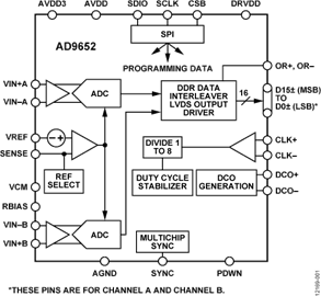
The dual ADC cores feature a multistage, pipelined architecture with integrated output error correction logic. A high performance on-chip buffer and internal voltage reference simplify the inter-face to external driving circuitry while preserving the exceptional performance of the ADC.
The AD9652 can support input clock frequencies of up to 1.24 GHz with a 1, 2, 4, and 8 integer clock divider used to generate the ADC sample clock. A duty cycle stabilizer is provided to compensate for variations in the ADC clock duty cycle. The 16-bit output data (with an overrange bit) from each ADC is interleaved onto a single LVDS output port along with a double data rate (DDR) clock. Programming for setup and control are accomplished using a 3-wire SPI-compatible serial interface.
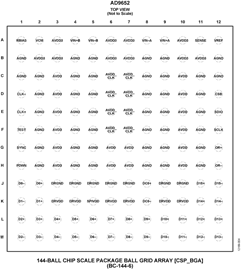
The AD9652 is available in a 144-ball CSP_BGA and is specified over the industrial temperature range of −40°C to +85°C. This product is protected by pending U.S. patents.
PRODUCT HIGHLIGHTS
- Integrated dual, 16-bit, 310 MSPS ADCs.
- On-chip buffer simplifies ADC driver interface.
- Operation from a 3.3 V and 1.8 V supply and a separate digital
output driver supply accommodating LVDS outputs. - Proprietary differential input maintains excellent SNR
performance for input frequencies of up to 485 MHz. - SYNC input allows synchronization of multiple devices.
- Three-wire, 3.3 V or 1.8 V SPI port for register programming
and readback.
APPLICATIONS
- Miltary radar and communications
- Multimode digital receivers (3G or 4G)
- Test and Instrumentation
- Smart antenna systems
This product has been released to the market. The data sheet contains all final specifications and operating conditions. For new designs, ADI recommends utilization of these products.


