
- Manufacturer Part Number : LTC2185
- Manufacturer : AD
- Description : 16-Bit, 125Msps Low Power Dual ADCs
- Series : LTC2185
- Reference Price : USD 81.6
- Our Price : We have a better price, contact us by email
- Product Type : High Speed A/D Converters >10 MSPS
- Function : Standard High Speed A/D Converters >20 MSPS
- Current Suggest : Production
- Status : Production
- RoHS Status: -
- Voltage: -
- Feature: -
- Package Case: -
- Temperature Range: -
- Packing: Reel/Tray/Tube
- Standard Packing Quantity: -
- Country of Origin: -
- Other Part Number : LTC2185
- Shipping methods : DHL FEDEX UPS TNT
- Delivery Time : Ship within 1 day.
- Manufacturer Production time : 6-8 weeks (Normally have stocks)
- Weight : 0.001KG
Contact us to check the best price and real time inventory quantity for LTC2185. If you need any more information about LTC2185, you can also send us by email. Our email is [email protected], we will reply you in 12 hours.
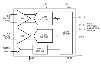
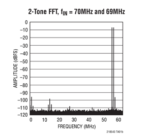
The LTC2185/LTC2184/LTC2183 are two-channel simultaneous sampling 16-bit A/D converters designed for digitizing high frequency, wide dynamic range signals. They are perfect for demanding communications applications with AC performance that includes 76.8dB SNR and 90dB spurious free dynamic range (SFDR). Ultralow jitter of 0.07psRMS allows undersampling of IF frequencies with excellent noise performance.
DC specs include ±2LSB INL (typ), ±0.5LSB DNL (typ) and no missing codes over temperature. The transition noise is 3.4LSBRMS.
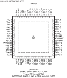
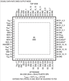
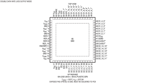
The digital outputs can be either full rate CMOS, Double Data Rate CMOS, or Double Data Rate LVDS. A separate output power supply allows the CMOS output swing to range from 1.2V to 1.8V.
The ENC+ and ENC– inputs may be driven differentially or single-ended with a sine wave, PECL, LVDS, TTL, or CMOS inputs. An optional clock duty cycle stabilizer allows high performance at full speed for a wide range of clock duty cycles.
Applications
- Communications
- Cellular Base Stations
- Software Defined Radios
- Portable Medical Imaging
- Multi-Channel Data Acquisition
- Nondestructive Testing
At least one model within this product family is in production and available for purchase. The product is appropriate for new designs but newer alternatives may exist.
