
- Manufacturer Part Number : LTM2173HY-14#PBF
- Manufacturer : AD
- Description : 14-Bit, 80Msps Low Power Quad ADC IC
- Series : LTM2173-14
- Reference Price : USD 60
- Our Price : We have a better price, contact us by email
- Product Type : Integrated/Special Purpose A/D Converters
- Function : Signal Chain μModule Receivers
- Current Suggest : Recommended for New Designs
- Status : Production
- ROHS Status : ROHS Compliant (Lead Free)
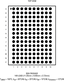
- Package Type : 140-Lead BGA (11.25mm x 9mm x 2.72mm)
- Pins : 140
- MFG Package Case : 05-08-1849
- Part Type : OTH
- Standard Packing Type : Tray
- Standard Packing Quantity : 210
- Working Temperature : -40 to 105C
- Other Part Number : LTM2173HY-14#PBF
- Shipping methods : DHL FEDEX UPS TNT
- Delivery Time : Ship within 1 day.
- Manufacturer Production time : 6-8 weeks (Normally have stocks)
- Weight : 0.001KG
Contact us to check the best price and real time inventory quantity for LTM2173HY-14#PBF. If you need any more information about LTM2173HY-14#PBF, you can also send us by email. Our email is [email protected], we will reply you in 12 hours.
- 4-Channel Simultaneous Sampling ADC
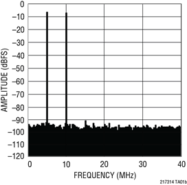
- 73dB SNR
- 88dB SFDR
- Low Power: 96mW per Channel
- Single 1.8V Supply
- Serial LVDS Outputs: 1 or 2 Bits per Channel
- Selectable Input Ranges: 1VP-P to 2VP-P
- 800MHz Full Power Bandwidth S/H
- Shutdown and Nap Modes
- Serial SPI Port for Configuration
- Internal Bypass Capacitance, No External Components
- 140-Pin (11.25mm × 9mm) BGA Package
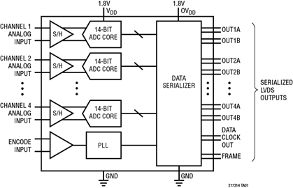
The LTM2173-14 is a 4-channel, simultaneous sampling 14-bit A/D converter designed for digitizing high frequency, wide dynamic range signals. AC performance includes 73dB SNR and 88dB spurious free dynamic range (SFDR). Low power consumption per channel reduces heat in high channel count applications. Integrated bypass capacitance and flow-through pinout reduces overall board space requirements.
DC specs include ±1LSB INL (typ), ±0.3LSB DNL (typ) and no missing codes over temperature. The transition noise is a low 1.2LSBRMS.
The digital outputs are serial LVDS to minimize the number of data lines. Each channel outputs two bits at a time (2-lane mode). At lower sampling rates there is a one bit per channel option (1-lane mode).
The ENC+ and ENC– inputs may be driven differentially or single-ended with a sine wave, PECL, LVDS, TTL, or CMOS inputs. An internal clock duty cycle stabilizer allows high performance at full speed for a wide range of clock duty cycles.
Applications
- Automotive
- Communications
- Cellular Base Stations
- Software Defined Radios
- Portable Medical Imaging
- Multichannel Data Acquisition
- Nondestructive Testing
This product has been released to the market. The data sheet contains all final specifications and operating conditions. For new designs, ADI recommends utilization of these products.


