
- Manufacturer Part Number : AD605ACHIPS
- Manufacturer : AD
- Description : Dual, Low Noise, Single-Supply Variable Gain Amplifier IC
- Series : AD605
- Reference Price : USD 0
- Our Price : We have a better price, contact us by email
- Product Type : Variable Gain Amplifiers (VGA)
- Function : Analog Control VGAs
- Current Suggest : Production
- Status : Contact ADI
- ROHS Status : ROHS Compliant (Lead Free)
- Package Type : CHIPS OR DIE
- Pins : 0
- MFG Package Case : X
- Part Type : REEL
- Standard Packing Type : Tray
- Standard Packing Quantity : 140
- Working Temperature : 25C
- Other Part Number : AD605ACHIPS
- Shipping methods : DHL FEDEX UPS TNT
- Delivery Time : Ship within 1 day.
- Manufacturer Production time : 6-8 weeks (Normally have stocks)
- Weight : 0.001KG
Contact us to check the best price and real time inventory quantity for AD605ACHIPS. If you need any more information about AD605ACHIPS, you can also send us by email. Our email is [email protected], we will reply you in 12 hours.
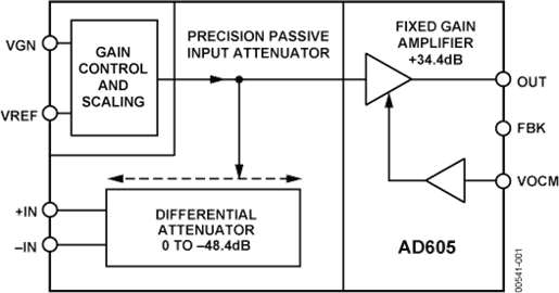
The high performance linear-in-dB response of the AD605 is achieved with the differential input, single-supply, exponential amplifier (DSX-AMP) architecture. Each of the DSX-AMPs comprises a variable attenuator of 0 dB to −48.4 dB followed by a high speed, fixed-gain amplifier. The attenuator is based on a 7-stage R-1.5R ladder network. The attenuation between tap points is 6.908 dB, and 48.360 dB for the entire ladder network. The DSX-AMP architecture results in 1.8 nV/√Hz input noise spectral density and accepts a ±2.0 V input signal when VOCM is biased at VP/2.
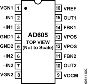
Each independent channel of the AD605 provides a gain range of 48 dB that can be optimized for the application. Gain ranges between −14 dB to +34 dB and 0 dB to +48 dB can be selected by a single resistor between Pin FBK and Pin OUT. The lower and upper gain ranges are determined by shorting Pin FBK to Pin OUT or leaving Pin FBK unconnected, respectively. The two channels of the AD605 can be cascaded to provide 96 dB of very accurate gain range in a monolithic package.
The gain control interface provides an input resistance of approximately 2 MΩ and scale factors from 20 dB/V to 30 dB/V for a VREF input voltage of 2.5 V to 1.67 V, respectively. Note that scale factors up to 40 dB/V are achievable with reduced accuracy for scales above 30 dB/V. The gain scales linearly in dB with control voltages (VGN) of 0.4 V to 2.4 V for the 20 dB/V scale and 0.20 V to 1.20 V for the 40 dB/V scale. When VGN is <50 mV, the amplifier is powered down to draw 1.9 mA. Under normal operation, the quiescent supply current of each amplifier channel is only 18 mA.
The AD605 is available in a 16-lead PDIP and a 16-lead SOIC_N package and is guaranteed for operation over the −40°C to +85°C temperature range.
Applications
Data Sheet, Rev. E, 5/07
At least one model within this product family is in production and available for purchase. The product is appropriate for new designs but newer alternatives may exist.


