
- Manufacturer Part Number : AD8330ARQZ-RL
- Manufacturer : AD
- Description : Low Cost, DC to 150 MHz, Variable Gain Amplifier IC
- Series : AD8330
- Reference Price : USD 3.624
- Our Price : We have a better price, contact us by email
- Product Type : Variable Gain Amplifiers (VGA)
- Function : Analog Control VGAs
- Current Suggest : Production
- Status : Production
- ROHS Status : ROHS Compliant (Lead Free)
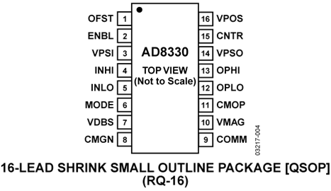
- Package Type : 16-Lead QSOP
- Pins : 16
- MFG Package Case : RQ-16
- Part Type : REEL
- Standard Packing Type : Reel
- Standard Packing Quantity : 2500
- Working Temperature : -40 to 85C
- Other Part Number : AD8330ARQZ-RL
- Shipping methods : DHL FEDEX UPS TNT
- Delivery Time : Ship within 1 day.
- Manufacturer Production time : 6-8 weeks (Normally have stocks)
- Weight : 0.001KG
Contact us to check the best price and real time inventory quantity for AD8330ARQZ-RL. If you need any more information about AD8330ARQZ-RL, you can also send us by email. Our email is [email protected], we will reply you in 12 hours.
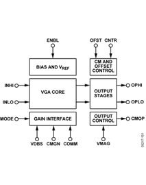
The AD8330 is a wideband variable gain amplifier for applicationsrequiring a fully differential signal path, low noise, well-definedgain, and moderately low distortion, from dc to 150 MHz. Theinput pins can also be driven from a single-ended source. Thepeak differential input is ±2 V, allowing sine wave operation at1 V rms with generous headroom. The output pins can drivesingle-sided loads essentially rail-to-rail. The differential outputresistance is 150 Ω. The output swing is a linear function of thevoltage applied to the VMAG pin that internally defaults to 0.5 V,providing a peak output of ±2 V. This can be raised to 10 V p-p,limited by the supply voltage.
The basic gain function is linear-in-dB, controlled by the voltageapplied to Pin VDBS. The gain ranges from 0 dB to 50 dB forcontrol voltages between 0 V and 1.5 V—a slope of 30 mV/dB.The gain linearity is typically within ±0.1 dB. By changing thelogic level on Pin MODE, the gain decreases over the same range,with an opposite slope. A second gain control port is providedat the VMAG pin and allows the user to vary the numeric gainfrom a factor of 0.03 to 10. All the parameters of the AD8330have low sensitivities to temperature and supply voltages. UsingVMAG, the basic 0 dB to 50 dB range can be repositioned toany value from 20 dB higher (that is, 20 dB to 70 dB) to at least30 dB lower (that is, –30 dB to +20 dB) to suit the application,thereby providing an unprecedented gain range of over 100 dB.A unique aspect of the AD8330 is that its bandwidth and pulseresponse are essentially constant for all gains, over both thebasic 50 dB linear-in-dB range, but also when using the linearin-magnitudefunction. The exceptional stability of the HFresponse over the gain range is of particular value in those VGAapplications where it is essential to maintain accurate gain lawconformanceat high frequencies.
An external capacitor at Pin OFST sets the high-pass corner ofan offset reduction loop, whose frequency can be as low as 5 Hz.When this pin is grounded, the signal path becomes dc-coupled.When used to drive an ADC, an external common-mode controlvoltage at Pin CNTR can be driven to within 0.5 V of either groundor VS to accommodate a wide variety of requirements. By default,the two outputs are positioned at the midpoint of the supply, VS/2.Other features, such as two levels of power-down (fully off anda hibernate mode), further extend the practical value of thisexceptionally versatile VGA.
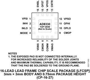
The AD8330 is available in 16-lead LFCSP and 16-lead QSOPpackages and is specified for operation from −40°C to +85°C.
Applications
- Pre-ADC signal conditioning
- 75 Ω cable driving adjust
- AGC amplifiers
At least one model within this product family is in production and available for purchase. The product is appropriate for new designs but newer alternatives may exist.


