
- Manufacturer Part Number : AD8372
- Manufacturer : AD
- Description : 41 dB Range, 1 dB Step Size, Programmable Dual VGA
- Series : AD8372
- Reference Price : USD 5.264
- Our Price : We have a better price, contact us by email
- Product Type : Variable Gain Amplifiers (VGA)
- Function : Digital Control VGAs
- Current Suggest : Recommended for New Designs
- Status : Production
- RoHS Status: -
- Voltage: -
- Feature: -
- Package Case: -
- Temperature Range: -
- Packing: Reel/Tray/Tube
- Standard Packing Quantity: -
- Country of Origin: -
- Other Part Number : AD8372
- Shipping methods : DHL FEDEX UPS TNT
- Delivery Time : Ship within 1 day.
- Manufacturer Production time : 6-8 weeks (Normally have stocks)
- Weight : 0.001KG
Contact us to check the best price and real time inventory quantity for AD8372. If you need any more information about AD8372, you can also send us by email. Our email is [email protected], we will reply you in 12 hours.
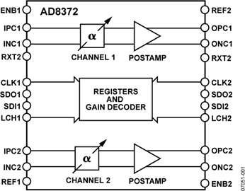
The AD8372 is a dual, digitally controlled, variable gainamplifier (VGA) that provides precise gain control, high IP3,and low noise figure. The excellent distortion performance andmoderate signal bandwidth make the AD8372 a suitable gain control device for a variety of multichannel receiverapplications.
For wide input dynamic range applications, the AD8372provides a broad 41 dB gain range. The gain is programmedthrough a bidirectional 4-pin serial interface. The serial interface consists of a clock, latch, data input, and data output linesfor each channel.
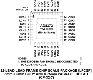
The AD8372 provides the ability to set the transconductance of the output stage using a single external resistor. The RXT1 and RXT2 pins provide a band gap derived stable reference voltage of 1.56 V. Typically 2.0 kΩ shunt resistors to ground are used toset the maximum gain to a nominal value of 31 dB. The currentsetting resistors can be adjusted to manipulate the gain anddistortion performance of each channel. This is a flexible feature in applications where it is desirable to trade off distortion performance for lower power consumption.
The AD8372 is powered on by applying the appropriate logiclevel to the ENB1, ENB2 pins. When powered down, the AD8372consumes less than 2.6 mA and offers excellent input-to-outputisolation. The gain setting is preserved when powered down.
Fabricated on an Analog Devices, Inc., high frequency BiCMOS process, the AD8372 provides precise gain adjustment capabilities with good distortion performance. The quiescent current of theAD8372 is typically 106 mA per channel. The AD8372 amplifier comes in a compact, thermally enhanced 5 mm × 5 mm 32-leadLFCSP package and operates over the temperature range of −40°C to +85°C.
Applications
- Differential ADC drivers
- CMTS upstream direct sampling receivers
- CATV modem signal scaling
- Generic RF/IF gain stages
- Single-ended-to-differential conversion
This product has been released to the market. The data sheet contains all final specifications and operating conditions. For new designs, ADI recommends utilization of these products.


