
- Manufacturer Part Number : ADL5330ACPZ-R2
- Manufacturer : AD
- Description : 10 MHz to 3 GHz VGA with 60 dB Gain Control Range IC
- Series : ADL5330
- Reference Price : USD 4.448
- Our Price : We have a better price, contact us by email
- Product Type : Variable Gain Amplifiers (VGA)
- Function : Analog Control VGAs
- Current Suggest : Recommended for New Designs
- Status : Production
- ROHS Status : ROHS Compliant (Lead Free)
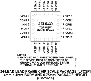
- Package Type : 24-Lead LFCSP (4mm x 5mm w/ EP)
- Pins : 24
- MFG Package Case : CP-24-14
- Part Type : REEL
- Standard Packing Type : Reel
- Standard Packing Quantity : 250
- Working Temperature : -40 to 85C
- Other Part Number : ADL5330ACPZ-R2
- Shipping methods : DHL FEDEX UPS TNT
- Delivery Time : Ship within 1 day.
- Manufacturer Production time : 6-8 weeks (Normally have stocks)
- Weight : 0.001KG
Contact us to check the best price and real time inventory quantity for ADL5330ACPZ-R2. If you need any more information about ADL5330ACPZ-R2, you can also send us by email. Our email is [email protected], we will reply you in 12 hours.
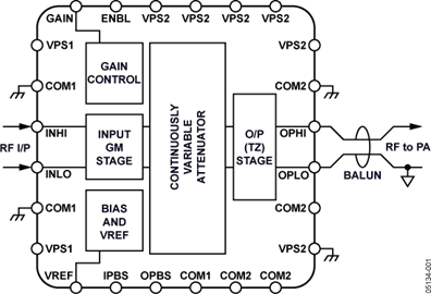
The ADL5330 is a high performance, voltage controlled, variablegain amplifier (VGA)/attenuator for use in applications withfrequencies up to 3 GHz. The balanced structure of the signalpath minimizes distortion while it also reduces the risk ofspurious feedforward at low gains and high frequencies causedby parasitic coupling. While operation between a balanced sourceand load is recommended, a single sided input is internallyconverted to differential form.
The input impedance is 50 Ω from INHI to INLO. The outputsare usually coupled into a 50 Ω grounded load via a 1:1 balun. Asingle supply of 4.75 V to 5.25 V is required.
The 50 Ω input system converts the applied voltage to a pair ofdifferential currents with high linearity and good commonrejection even when driven by a single sided source. The signalcurrents are then applied to a proprietary voltage controlledattenuator providing precise definition of the overall gain underthe control of the linear in dB interface. The GAIN pin accepts avoltage from 0 V at minimum gain to 1.4 V at full gain with a20 mV/dB scaling factor.
The output of the high accuracy wideband attenuator is appliedto a differential transimpedance output stage. The output stagesets the 50 Ω differential output impedances and drives theOPHI and OPLO pins. The ADL5330 has a power-downfunction. It can be powered down by a Logic LO input on theENBL pin. The current consumption in power-down mode is250 μA.
The ADL5330 is fabricated on an Analog Devices, Inc.,proprietary high performance, complementary bipolar IC process.The ADL5330 is available in a 24-lead (4 mm × 4 mm), Pb-freeLFCSP package and is specified for operation from ambienttemperatures of −40°C to +85°C. An evaluation board is alsoavailable.
Applications
- Transmit and receive power control at RF and IF
This product has been released to the market. The data sheet contains all final specifications and operating conditions. For new designs, ADI recommends utilization of these products.


