
- Manufacturer Part Number : ADL5331ACPZ-R7
- Manufacturer : AD
- Description : 1 MHz to 1.2 GHz VGA with 30 dB Gain Control Range IC
- Series : ADL5331
- Reference Price : USD 4.128
- Our Price : We have a better price, contact us by email
- Product Type : Variable Gain Amplifiers (VGA)
- Function : Analog Control VGAs
- Current Suggest : Recommended for New Designs
- Status : Production
- ROHS Status : ROHS Compliant (Lead Free)
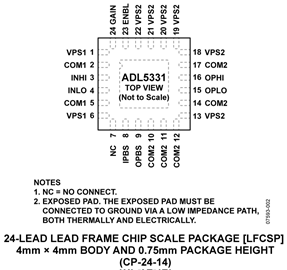
- Package Type : 24-Lead LFCSP (4mm x 5mm w/ EP)
- Pins : 24
- MFG Package Case : CP-24-14
- Part Type : REEL
- Standard Packing Type : Reel
- Standard Packing Quantity : 1500
- Working Temperature : -40 to 85C
- Other Part Number : ADL5331ACPZ-R7
- Shipping methods : DHL FEDEX UPS TNT
- Delivery Time : Ship within 1 day.
- Manufacturer Production time : 6-8 weeks (Normally have stocks)
- Weight : 0.001KG
Contact us to check the best price and real time inventory quantity for ADL5331ACPZ-R7. If you need any more information about ADL5331ACPZ-R7, you can also send us by email. Our email is [email protected], we will reply you in 12 hours.
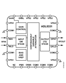
The ADL5331 is a high performance, voltage-controlledvariable gain amplifier/attenuator for use in applications with frequencies up to 1.2 GHz. The balanced structure of the signal path maximizes signal swing, eliminates common-mode noiseand minimizes distortion while it also reduces the risk of spurious feed-forward at low gains and high frequencies caused by parasitic coupling.
The 50 Ω differential input system converts the applieddifferential voltage at INHI and INLO to a pair of differentialcurrents with high linearity and good common-mode rejection. The signal currents are then applied to a proprietary voltage-controlled attenuator providing precise definition of the overall gain under the control of the linear-in-dB interface. The GAIN pin accepts a voltage from 0 V at a minimum gain to 1.4 V at afull gain with a 40 mV/dB scaling factor over most of the range.
The output of the high accuracy wideband attenuator is appliedto a differential transimpedance output stage. The output stageprovides a differential output at OPHI and OPLO, which must be pulled up to the supply with RF chokes or a center-tapped balun.
The ADL5331 consumes 240 mA of current including the output pins and operates off a single supply ranging from 4.75 V to 5.25 V. A power-down function is provided by applying alogic low input on the ENBL pin. The current consumption inpower-down mode is 250 μA.
The ADL5331 is fabricated on an Analog Devices, Inc., proprietary high performance, complementary bipolar IC process.The ADL5331 is available in a 24-lead (4 mm × 4 mm), Pb-freeLFCSP package and is specified for operation from ambient temperatures of −40°C to +85°C. An evaluation board is also available.
Applications
- Transmit and receive power control at RF and IF
- CATV distribution
This product has been released to the market. The data sheet contains all final specifications and operating conditions. For new designs, ADI recommends utilization of these products.


