
- Manufacturer Part Number : AD-FMCOMMS11-EBZ
- Manufacturer : AD
- Description : Dual, 35 dB Range, 1 dB Step Size DGA IC
- Series : ADL5205
- Reference Price : USD 0
- Our Price : We have a better price, contact us by email
- Product Type : Variable Gain Amplifiers (VGA)
- Function : Digital Control VGAs
- Current Suggest : Recommended for New Designs
- Status : Production
- ROHS Status : ROHS Compliant (Lead Free)
- Package Type : Direct RF to Baseband 5GHz Radio
- Pins : -
- MFG Package Case : -
- Part Type : EVAL
- Standard Packing Type : -
- Standard Packing Quantity : -
- Working Temperature : -
- Other Part Number : AD-FMCOMMS11-EBZ
- Shipping methods : DHL FEDEX UPS TNT
- Delivery Time : Ship within 1 day.
- Manufacturer Production time : 6-8 weeks (Normally have stocks)
- Weight : 0.001KG
Contact us to check the best price and real time inventory quantity for AD-FMCOMMS11-EBZ. If you need any more information about AD-FMCOMMS11-EBZ, you can also send us by email. Our email is [email protected], we will reply you in 12 hours.
- Dual, independent, digitally controlled gain amplifier (DGA)
- −9 dB to +26 dB gain range
- 1 dB step size, ±0.2 dB accuracy at 200 MHz
- 100 Ω differential input resistance
- 10 Ω differential output resistance
- 1.2 dB change in noise figure for first 12 dB of gain reduction
- Output third-order intercept (OIP3): 48.5 dBm at 200 MHz, 5 V, high performance mode
- −3 dB bandwidth: 1700 MHz typical in high performance mode
- Multiple control interface options
- Parallel 6-bit control interface with latch
- Serial peripheral interface (SPI) with fast attack
- Gain step up/down interface
- Wide input dynamic range
- Low power mode
- Power-down control
- Single 3.3 V or 5 V supply operation
- 40-lead, 6 mm × 6 mm LFCSP package
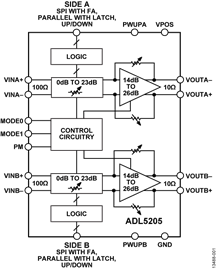
The ADL5205 is a digitally controlled, wide bandwidth, variable gain dual amplifier (DGA) that provides precise gain control, high output third-order intercept (OIP3) and a near constant noise figure for the first 12 dB of attenuation. The excellent OIP3 performance of 48.5 dBm (at 200 MHz, 5 V, high performance mode, and maximum gain) makes the ADL5205 an excellent gain control device for a variety of receiver applications.
For wide input dynamic range applications, the ADL5205 provides a broad 35 dB gain range with a 1 dB step size. The gain is adjustable through multiple gain control and interface options: parallel, SPI, or gain step up/down control.
The two channels of the ADL5205 can be powered up independently by applying the appropriate logic level to the PWUPA and PWUPB pins. The quiescent current of the ADL5205 is typically 175 mA for high performance mode and 135 mA for low power mode. When disabled, the ADL5205 consumes only 14 mA and offers excellent input to output isolation. The gain setting is preserved when the device is disabled.
Fabricated on the Analog Devices, Inc., high speed, silicon germanium (SiGe) complementary BiCMOS process, the ADL5205 provides precise gain adjustment capabilities with good distortion performance. The ADL5205 amplifier comes in a compact, thermally enhanced, 6 mm × 6 mm, 40-lead LFCSP package and operates over the temperature range of −40°C to +85°C.
Note that throughout this data sheet, multifunction pins, such as CSA/A3, are referred to by the entire pin name or by a single function of the pin, for example, CSA, when only that function is relevant.
Applications
- Differential analog-to-digital converter (ADC) drivers
- High intermediate frequency (IF) sampling receivers
- High output power IF amplification
- Instrumentation
This product has been released to the market. The data sheet contains all final specifications and operating conditions. For new designs, ADI recommends utilization of these products.


