
- Manufacturer Part Number : ADCMP605BCPZ-WP
- Manufacturer : AD
- Description : Rail-to-Rail, Very Fast, 2.5 V to 5.5 V, Single-Supply LVDS Comparator in a 12-lead LSCFP Package IC
- Series : ADCMP605
- Reference Price : USD 1.904
- Our Price : We have a better price, contact us by email
- Product Type : Comparators
- Function : High Speed Comparators (<100ns Propagation Delay)
- Current Suggest : Production
- Status : Production
- ROHS Status : ROHS Compliant (Lead Free)
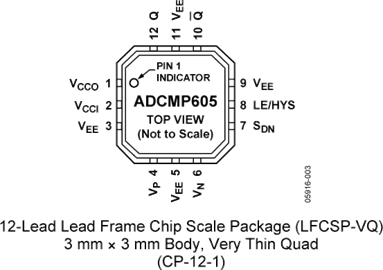
- Package Type : 12-Lead LFCSP (3mm x 3mm)
- Pins : 12
- MFG Package Case : CP-12-1
- Part Type : REEL
- Standard Packing Type : Tray
- Standard Packing Quantity : 50
- Working Temperature : -40 to 125C
- Other Part Number : ADCMP605BCPZ-WP
- Shipping methods : DHL FEDEX UPS TNT
- Delivery Time : Ship within 1 day.
- Manufacturer Production time : 6-8 weeks (Normally have stocks)
- Weight : 0.001KG
Contact us to check the best price and real time inventory quantity for ADCMP605BCPZ-WP. If you need any more information about ADCMP605BCPZ-WP, you can also send us by email. Our email is [email protected], we will reply you in 12 hours.
- Fully specified rail to rail at VCCI = 2.5 V to 5.5 V
- Input common-mode voltage from −0.2 V to VCCI + 0.2 V
- Low glitch LVDS-compatible output stage
- 1.6 ns propagation delay
- 37 mW at 2.5 V
- Shutdown pin
- Single-pin control for programmable hysteresis and latch
- Power supply rejection > 60 dB
- −40°C to +125°C operation
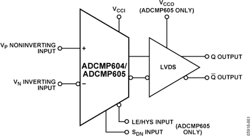
The ADCMP604/ADCMP605 are very fast comparators fabricated on the Analog Devices, Inc. proprietary XFCB2 process. These comparators are exceptionally versatile and easy to use. Features include an input range from VEE − 0.5 V to VCCI + 0.2 V, low noise, LVDS-compatible output drivers, and TTL/CMOS latch inputs with adjustable hysteresis and/or shut-down inputs.
The devices offer 1.5 ns propagation delays with 1 ps rms random jitter (RJ). Overdrive and slew rate dispersion are typically less than 50 ps.A flexible power supply scheme allows the devices to operate with a single 2.5 V positive supply and a −0.5 V to +2.7 V input signal range up to a 5.5 V positive supply with a −0.5 V to +5.7 V input signal range. Split input/output supplies, with no sequencing restrictions on the ADCMP605, support a wide input signal range with greatly reduced power consumption.
The LVDS-compatible output stage is designed to drive any standard LVDS input. The comparator input stage offers robust protection against large input overdrive, and the outputs do not phase reverse when the valid input signal range is exceeded. High speed latch and programmable hysteresis features are also provided in a unique single-pin control option.
The ADCMP604 is available in a 6-lead SC70 package, and the ADCMP605 is available in a 12-lead LFCSP.
Applications
- High speed instrumentation
- Clock and data signal restoration
- Logic level shifting or translation
- Pulse spectroscopy
- High speed line receivers
- Threshold detection
- Peak and zero-crossing detectors
- High speed trigger circuitry
- Pulse-width modulators
- Current-/voltage-controlled oscillators
- Automatic test equipment (ATE)
At least one model within this product family is in production and available for purchase. The product is appropriate for new designs but newer alternatives may exist.


