
- Manufacturer Part Number : SSM4321
- Manufacturer : AD
- Description : Mono 2.9 W Class-D Audio Amplifier with Digital Current and Voltage Output
- Series : SSM4321
- Reference Price : USD 0
- Our Price : We have a better price, contact us by email
- Product Type : Audio Amplifiers
- Function : Class-D Audio Amplifiers
- Current Suggest : Not Recommended for New Designs
- Status : Production
- RoHS Status: -
- Voltage: -
- Feature: -
- Package Case: -
- Temperature Range: -
- Packing: Reel/Tray/Tube
- Standard Packing Quantity: -
- Country of Origin: -
- Other Part Number : SSM4321
- Shipping methods : DHL FEDEX UPS TNT
- Delivery Time : Ship within 1 day.
- Manufacturer Production time : 6-8 weeks (Normally have stocks)
- Weight : 0.001KG
Contact us to check the best price and real time inventory quantity for SSM4321. If you need any more information about SSM4321, you can also send us by email. Our email is [email protected], we will reply you in 12 hours.
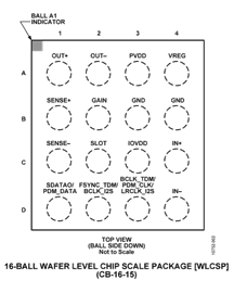
The SSM4321 is a fully integrated, high efficiency, Class-Daudio amplifier with digitized output of output voltage, outputcurrent, and the PVDD supply voltage. It is designed to maximize performance for mobile phone applications. The application circuit requires a minimum of external components and operates from a 2.5 V to 5.5 V supply for the amplifier and a 1.42 V to 3.6 V supply for input/output. The SSM4321 is capable of delivering 2.2 W of continuous output power with <1% THD + N driving a 4 Ω load from a 5.0 V supply with a 0.1 Ω V/I sense resistor.
The SSM4321 features a high efficiency, low noise modulation scheme that requires no external LC output filters. The modulation scheme provides high efficiency even at low output power. The SSM4321 operates with 89% efficiency at 1.4 W into 8 Ω from a 5.0 V supply with an SNR of >100 dB.
The SSM4321 includes circuitry to sense output current, output voltage, and the PVDD supply voltage. Current sense is performedusing an external sense resistor that is connected between anoutput pin and the load. The output current and voltage are sentto ADCs with 16-bit resolution; the PVDD supply voltage is sent to an ADC with 8-bit resolution.
The outputs of these ADCs are available on the TDM or I2S output serial port. The SLOT pin is used to determine which of four possible output slots is used on the TDM interface. A stereo I2S interface can be selected by reversing the pin connections forBCLK and FSYNC. Also, a direct PDM bit stream of voltage andcurrent data can be selected via the SLOT pin.
Spread-spectrum pulse density modulation (PDM) is used to provide lower EMI-radiated emissions compared with other Class-D architectures. The inherent randomized nature of spread-spectrum PDM eliminates the clock intermodulation (beating effect) of several amplifiers in close proximity.
The SSM4321 produces ultralow EMI emissions that significantlyreduce the radiated emissions at the Class-D outputs, particularly above 100 MHz. The ultralow EMI emissions of the SSM4321 arealso helpful for antenna and RF sensitivity problems.
The device includes a highly flexible gain select pin that requiresonly one series resistor to select a gain setting of 0 dB, 3 dB, 6 dB, 9 dB, or 12 dB. Input impedance is fixed at 80 kΩ, independent of the selected gain.
The SSM4321 has a shutdown mode with a typical shutdowncurrent of <1 μA. Shutdown is enabled by removing the BCLK input. A clock must be present on the BCLK pin for the part to operate. The device also includes pop-and-click suppression circuitry, which minimizes voltage glitches at the output during turn-on and turn-off, reducing audible noise on activation and deactivation.
The SSM4321 is specified over the industrial temperature rangeof −40°C to +85°C. It has built-in thermal shutdown and output short-circuit protection. It is available in a halide-free, 16-ball, 0.4 mm pitch, 1.74 mm × 1.74 mm wafer level chip scale package (WLCSP).
Applications
- Mobile phones
- MP3 players
- Portable electronics
This designates products ADI does not recommend broadly for new designs.


