
- Manufacturer Part Number : AD9511BCPZ
- Manufacturer : AD
- Description : 1.2 GHz Clock Distribution IC, PLL Core, Dividers, Delay Adjust, Five Outputs IC
- Series : AD9511
- Reference Price : USD 5.432
- Our Price : We have a better price, contact us by email
- Product Type : Clock Generation & Distribution
- Function : Clock Generation Devices
- Current Suggest : Recommended for New Designs
- Status : Production
- ROHS Status : ROHS Compliant (Lead Free)
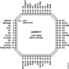
- Package Type : 48-Lead LFCSP (7mm x 7mm w/ EP)
- Pins : 48
- MFG Package Case : CP-48-1
- Part Type : OTH
- Standard Packing Type : Tray
- Standard Packing Quantity : 260
- Working Temperature : -40 to 85C
- Other Part Number : AD9511BCPZ
- Shipping methods : DHL FEDEX UPS TNT
- Delivery Time : Ship within 1 day.
- Manufacturer Production time : 6-8 weeks (Normally have stocks)
- Weight : 0.001KG
Contact us to check the best price and real time inventory quantity for AD9511BCPZ. If you need any more information about AD9511BCPZ, you can also send us by email. Our email is [email protected], we will reply you in 12 hours.
- Phase locked loop (PLL) Core
Reference input frequencies to 250 MHz
Programmable dual-modulus prescaler
Programmable charge pump (CP) current
Separate CP supply (VCP) extends tuning range - Two 1.6 GHz, differential clock inputs
- 5 programmable dividers, 1 to 32, all integers
- Phase select for output-to-output coarse delay adjust
- Three independent 1.2 GHz LVPECL outputs
Additive output jitter , 225 fs RMS - Two independent 800 MHz/250 MHz LVDS/CMOS outputs
Additive output jitter, 275 fs RMS
Fine delay adjust on one output, 5-bit delay words - 4-wire or 3-wire serial control port
- Space-saving 48-lead LFCSP
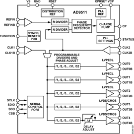
The PLL section consists of a programmable reference divider, R; a low-noise phase frequency detector, PFD; a precision charge pump, CP; and a programmable feedback divider, N. By connecting an external VCXO or VCO to the CLK2 and CLK2B pins, PLL output frequencies up to 1.6 GHz may be synchronized to the input reference, REFIN.
The clock distribution section provides LVPECL outputs and outputs that may be programmed to either LVDS or CMOS. Each output has a programmable divider, which may be bypassed or set to divide by any integer up to 32.
Each divider allows the user to change the phase of one clock output relative to another clock output. This phase select functions as a coarse timing adjustment. One output also features a programmable delay element with a user-selected, fullscale range to 10 ns. This fine tuning delay block is programmed with a 5-bit word, which gives the user 32 possible delays from which to choose.
The AD9511 is ideally suited for data converter clocking applications where maximum converter performance is achieved with sub-picosecond jitter encode signals.
The AD9511 is available in a 48-lead LFCSP and is specified from -40°C to +85°C. The part may be run from a single 3.3 V supply. Users wishing to extend the voltage range for external VCOs may run the charge pump supply, VCP, to 5.5V.
Applications
- Low jitter, low phase noise clock distribution
- Clocking high speed ADCs, DACs, DDS, DDC, DUC, MxFE™ Converters
- Wireless infrastructure transceivers
- High performance instrumentation
- Broadband infrastructure
This product has been released to the market. The data sheet contains all final specifications and operating conditions. For new designs, ADI recommends utilization of these products.


