
- Manufacturer Part Number : AD9511/PCB
- Manufacturer : AD
- Description : 1.2 GHz Clock Distribution IC, PLL Core, Dividers, Delay Adjust, Eight Outputs IC
- Series : AD9510
- Reference Price : USD 0
- Our Price : We have a better price, contact us by email
- Product Type : Clock Generation & Distribution
- Function : Clock Generation Devices
- Current Suggest : Recommended for New Designs
- Status : Obsolete
- ROHS Status : NON-ROHS Leaded
- Package Type : Evaluation Board
- Pins : -
- MFG Package Case : -
- Part Type : EVAL
- Standard Packing Type : -
- Standard Packing Quantity : -
- Working Temperature : -
- Other Part Number : AD9511/PCB
- Shipping methods : DHL FEDEX UPS TNT
- Delivery Time : Ship within 1 day.
- Manufacturer Production time : 6-8 weeks (Normally have stocks)
- Weight : 0.001KG
Contact us to check the best price and real time inventory quantity for AD9511/PCB. If you need any more information about AD9511/PCB, you can also send us by email. Our email is [email protected], we will reply you in 12 hours.
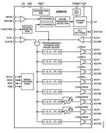
The AD9510 provides a multi-output clock distribution functionalong with an on-chip phase-locked loop (PLL) core. The designemphasizes low jitter and phase noise to maximize data converterperformance. Other applications with demanding phase noiseand jitter requirements also benefit from this device.
The PLL section consists of a programmable reference divider(R); a low noise, phase frequency detector (PFD); a precisioncharge pump (CP); and a programmable feedback divider (N).By connecting an external voltage-controlled crystal oscillator(VCXO) or voltage-controlled oscillator (VCO) to the CLK2and CLK2B pins, frequencies of up to 1.6 GHz can be synchronizedto the input reference.
There are eight independent clock outputs. Four outputs are lowvoltage positive emitter-coupled logic (LVPECL) at 1.2 GHz,and four are selectable as either LVDS (800 MHz) or CMOS(250 MHz) levels.
Each output has a programmable divider that can be bypassedor set to divide by any integer up to 32. The phase of one clockoutput relative to another clock output can be varied by meansof a divider phase select function that serves as a coarse timingadjustment. Two of the LVDS/CMOS outputs feature programmabledelay elements with full-scale ranges up to 8 ns of delay.This fine tuning delay block has 5-bit resolution, giving 25possible delays from which to choose for each full-scale setting(Register 0x36 and Register 0x3A = 00000b to 11000b).
The AD9510 is ideally suited for data converter clockingapplications where maximum converter performance isachieved by encode signals with subpicosecond jitter.
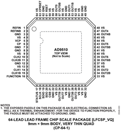
The AD9510 is available in a 64-lead LFCSP and can be operatedfrom a single 3.3 V supply. An external VCO, which requires anextended voltage range, can be accommodated by connectingthe charge pump supply (VCP) to 5.5 V. The temperature rangeis −40°C to +85°C.
Applications
- Low jitter, low phase noise clock distribution
- Clocking high speed ADCs, DACs, DDSs, DDCs, DUCs, and mixed-signal front ends (MxFEs)
- High performance wireless transceivers
- High performance instrumentation
- Broadband infrastructure
This product has been released to the market. The data sheet contains all final specifications and operating conditions. For new designs, ADI recommends utilization of these products.


