
- Manufacturer Part Number : AD9513
- Manufacturer : AD
- Description : 800 MHz Clock Distribution IC, Dividers, Delay Adjust, Three Outputs
- Series : AD9513
- Reference Price : USD 4.488
- Our Price : We have a better price, contact us by email
- Product Type : Clock Generation & Distribution
- Function : Clock Distribution Devices
- Current Suggest : Recommended for New Designs
- Status : Production
- RoHS Status: -
- Voltage: -
- Feature: -
- Package Case: -
- Temperature Range: -
- Packing: Reel/Tray/Tube
- Standard Packing Quantity: -
- Country of Origin: -
- Other Part Number : AD9513
- Shipping methods : DHL FEDEX UPS TNT
- Delivery Time : Ship within 1 day.
- Manufacturer Production time : 6-8 weeks (Normally have stocks)
- Weight : 0.001KG
Contact us to check the best price and real time inventory quantity for AD9513. If you need any more information about AD9513, you can also send us by email. Our email is [email protected], we will reply you in 12 hours.
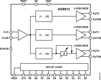
The AD9513 features a three-output clock distribution IC in adesign that emphasizes low jitter and phase noise to maximizedata converter performance. Other applications withdemanding phase noise and jitter requirements also benefitfrom this part.
There are three independent clock outputs that can be set toeither LVDS or CMOS levels. These outputs operate to 800MHz in LVDS mode and to 250 MHz in CMOS mode.
Each output has a programmable divider that can be set todivide by a selected set of integers ranging from 1 to 32. Thephase of one clock output relative to the other clock output canbe set by means of a divider phase select function that serves asa coarse timing adjustment.
One of the outputs features a delay element with three selectablefull-scale delay values (1.5 ns, 5 ns, and 10 ns), each with 16steps of fine adjustment.
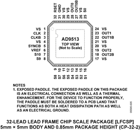
The AD9513 does not require an external controller foroperation or setup. The device is programmed by means of11 pins (S0 to S10) using 4-level logic. The programming pinsare internally biased to ⅓ VS. The VREF pin provides a level of⅔ VS. VS (3.3 V) and GND (0 V) provide the other two logic levels.
The AD9513 is ideally suited for data converter clockingapplications where maximum converter performance isachieved by encode signals with subpicosecond jitter.
The AD9513 is available in a 32-lead LFCSP and operates froma single 3.3 V supply. The temperature range is −40°C to +85°C.
Applications
- Low jitter, low phase noise clock distribution
- Clocking high speed ADCs, DACs, DDSs, DDCs, DUCs, MxFEs
- High performance wireless transceivers
- High performance instrumentation
- Broadband infrastructure
- ATE
This product has been released to the market. The data sheet contains all final specifications and operating conditions. For new designs, ADI recommends utilization of these products.


