Best Price NOW
Manufacturer / Brand: AD
Details: Low Jitter Clock Generator Eight LVPECL Outputs IC
Series: AD9525
Quantity Available: Over 60740 pieces
Datasheet for AD9525BCPZ:
Product Parameters
- Manufacturer Part Number : AD9525BCPZ
- Manufacturer : AD
- Description : Low Jitter Clock Generator Eight LVPECL Outputs IC
- Series : AD9525
- Reference Price : USD 6.664
- Our Price : We have a better price, contact us by email
- Product Type : Clock Generation & Distribution
- Function : Clock Generation Devices
- Current Suggest : Recommended for New Designs
- Status : Production
- ROHS Status : ROHS Compliant (Lead Free)
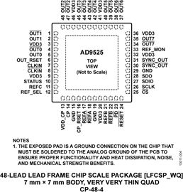
- Package Type : 48-Lead LFCSP (7mm x 7mm x 0.85mm w/ EP)
- Pins : 48
- MFG Package Case : CP-48-4
- Part Type : OTH
- Standard Packing Type : Tray
- Standard Packing Quantity : 260
- Working Temperature : -40 to 85C
- Other Part Number : AD9525BCPZ
- Shipping methods : DHL FEDEX UPS TNT
- Delivery Time : Ship within 1 day.
- Manufacturer Production time : 6-8 weeks (Normally have stocks)
- Weight : 0.001KG
Contact us to check the best price and real time inventory quantity for AD9525BCPZ. If you need any more information about AD9525BCPZ, you can also send us by email. Our email is [email protected], we will reply you in 12 hours.
Features and Benefits of AD9525BCPZ
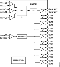
- Integrated ultra low noise synthesizer
- 8 differential 3.6 GHz LVPECL outputs and 1 LVPECL or 2 CMOS SYNC Outputs
- 2 differential reference inputs and 1 single-ended reference inputs
The AD9525 is designed to support converter clock requirements for long-term evolution (LTE) and multicarrier GSM base station designs.
The AD9525 provides a low power, multioutput, clock distribution function with low jitter performance, along with an on-chip PLL that can be used with an external VCO or VCXO. The VCO input and eight LVPECL outputs can operate up to a frequency of 3.6 GHz. All outputs share a common divider that can provide a division of 1 to 6.
The AD9525 offers a dedicated output that can be used to provide a programmable signal for resetting or synchronizing a data converter. The output signal is activated by a SPI write.
The AD9525 is available in a 48-lead LFCSP and can be operated from a single 3.3 V supply. The external VCXO or VCO can have an operating voltage of up to 5.5 V.
The AD9525 operates over the extended industrial temperature range of −40°C to +85°C.
Applications - LTE and multicarrier GSM base stations
- Clocking high speed ADCs, DACs
- ATE and high performance instrumentation
- 40/100Gb/s OTN Line Side Clocking
- Cable/DOCSIS CMTS Clocking
- Test and Measurement


