
- Manufacturer Part Number : ADCLK846
- Manufacturer : AD
- Description : 1.8 V, 6 LVDS/12 CMOS Outputs Low Power Clock Fanout Buffer
- Series : ADCLK846
- Reference Price : USD 3.2
- Our Price : We have a better price, contact us by email
- Product Type : Clock Generation & Distribution
- Function : Clock Distribution Devices
- Current Suggest : Recommended for New Designs
- Status : Production
- RoHS Status: -
- Voltage: -
- Feature: -
- Package Case: -
- Temperature Range: -
- Packing: Reel/Tray/Tube
- Standard Packing Quantity: -
- Country of Origin: -
- Other Part Number : ADCLK846
- Shipping methods : DHL FEDEX UPS TNT
- Delivery Time : Ship within 1 day.
- Manufacturer Production time : 6-8 weeks (Normally have stocks)
- Weight : 0.001KG
Contact us to check the best price and real time inventory quantity for ADCLK846. If you need any more information about ADCLK846, you can also send us by email. Our email is [email protected], we will reply you in 12 hours.
- Selectable LVDS/CMOS outputs
- Up to 6 LVDS (1.2 GHz) or 12 CMOS (250 MHz) outputs
- <16 mW per channel (100 MHz operation)
- 54 fs integrated jitter (12 kHz to 20 MHz)
- 100 fs additive broadband jitter
- 2.0 ns propagation delay (LVDS)
- 135 ps output rise/fall (LVDS)
- 65 ps output-to-output skew (LVDS)
- Sleep mode
- Pin-programmable control
- 1.8 V power supply
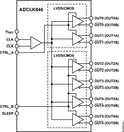
The ADCLK846 is a 1.2 GHz/250 MHz, LVDS/CMOS, fanout buffer optimized for low jitter and low power operation. Possible configurations range from 6 LVDS to 12 CMOS outputs, including combinations of LVDS and CMOS outputs. Two control lines are used to determine whether fixed blocks of outputs are LVDS or CMOS outputs.
The clock input accepts various types of single-ended and differential logic levels including LVPECL, LVDS, HSTL, CML, and CMOS.
Table 8 provides interface options for each type of connection. The SLEEP pin enables a sleep mode to power down the device.
This device is available in a 24-pin LFCSP package. It is specified for operation over the standard industrial temperature range of −40°C to +85°C.
Applications- Low jitter clock distribution
- Clock and data signal restoration
- Level translation
- Wireless communications
- Wired communications
- Medical and industrial imaging
- ATE and high performance instrumentation
This product has been released to the market. The data sheet contains all final specifications and operating conditions. For new designs, ADI recommends utilization of these products.


