
- Manufacturer Part Number : ADCLK854
- Manufacturer : AD
- Description : 1.8 V, 12-LVDS/24-CMOS Output, Low Power Clock Fanout Buffer
- Series : ADCLK854
- Reference Price : USD 3.8
- Our Price : We have a better price, contact us by email
- Product Type : Clock Generation & Distribution
- Function : Clock Distribution Devices
- Current Suggest : Recommended for New Designs
- Status : Production
- RoHS Status: -
- Voltage: -
- Feature: -
- Package Case: -
- Temperature Range: -
- Packing: Reel/Tray/Tube
- Standard Packing Quantity: -
- Country of Origin: -
- Other Part Number : ADCLK854
- Shipping methods : DHL FEDEX UPS TNT
- Delivery Time : Ship within 1 day.
- Manufacturer Production time : 6-8 weeks (Normally have stocks)
- Weight : 0.001KG
Contact us to check the best price and real time inventory quantity for ADCLK854. If you need any more information about ADCLK854, you can also send us by email. Our email is [email protected], we will reply you in 12 hours.
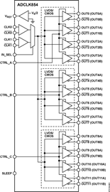
The ADCLK854 offers two selectable inputs and a sleep mode feature. The IN_SEL pin state determines which input is fanned out to all the outputs. The SLEEP pin enables a sleep mode to power down the device.
The inputs accept various types of single-ended and differential logic levels including LVPECL, LVDS, HSTL, CML, and CMOS. Table 8 provides interface options for each type of connection.
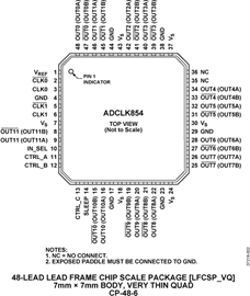
This device is available in a 48-pin LFCSP package. It is specified for operation over the standard industrial temperature range of −40°C to +85°C.
This product has been released to the market. The data sheet contains all final specifications and operating conditions. For new designs, ADI recommends utilization of these products.


