
- Manufacturer Part Number : ADCLK905/PCBZ
- Manufacturer : AD
- Description : 1.8 V, 12-LVDS/24-CMOS Output, Low Power Clock Fanout Buffer IC
- Series : ADCLK854
- Reference Price : USD 0
- Our Price : We have a better price, contact us by email
- Product Type : Clock Generation & Distribution
- Function : Clock Distribution Devices
- Current Suggest : Recommended for New Designs
- Status : Production
- ROHS Status : ROHS Compliant (Lead Free)
- Package Type : Evaluation Board
- Pins : -
- MFG Package Case : -
- Part Type : EVAL
- Standard Packing Type : -
- Standard Packing Quantity : -
- Working Temperature : -
- Other Part Number : ADCLK905/PCBZ
- Shipping methods : DHL FEDEX UPS TNT
- Delivery Time : Ship within 1 day.
- Manufacturer Production time : 6-8 weeks (Normally have stocks)
- Weight : 0.001KG
Contact us to check the best price and real time inventory quantity for ADCLK905/PCBZ. If you need any more information about ADCLK905/PCBZ, you can also send us by email. Our email is [email protected], we will reply you in 12 hours.
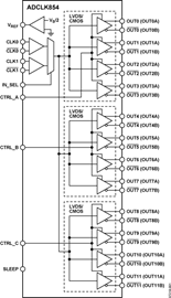
The ADCLK854 offers two selectable inputs and a sleep mode feature. The IN_SEL pin state determines which input is fanned out to all the outputs. The SLEEP pin enables a sleep mode to power down the device.
The inputs accept various types of single-ended and differential logic levels including LVPECL, LVDS, HSTL, CML, and CMOS. Table 8 provides interface options for each type of connection.
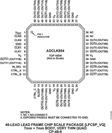
This device is available in a 48-pin LFCSP package. It is specified for operation over the standard industrial temperature range of −40°C to +85°C.
This product has been released to the market. The data sheet contains all final specifications and operating conditions. For new designs, ADI recommends utilization of these products.


