
- Manufacturer Part Number : ADCLK950
- Manufacturer : AD
- Description : Two Selectable Inputs, 10 LVPECL Outputs, SiGe Clock Fanout Buffer
- Series : ADCLK950
- Reference Price : USD 4.4
- Our Price : We have a better price, contact us by email
- Product Type : Clock Generation & Distribution
- Function : Clock Distribution Devices
- Current Suggest : Recommended for New Designs
- Status : Production
- RoHS Status: -
- Voltage: -
- Feature: -
- Package Case: -
- Temperature Range: -
- Packing: Reel/Tray/Tube
- Standard Packing Quantity: -
- Country of Origin: -
- Other Part Number : ADCLK950
- Shipping methods : DHL FEDEX UPS TNT
- Delivery Time : Ship within 1 day.
- Manufacturer Production time : 6-8 weeks (Normally have stocks)
- Weight : 0.001KG
Contact us to check the best price and real time inventory quantity for ADCLK950. If you need any more information about ADCLK950, you can also send us by email. Our email is [email protected], we will reply you in 12 hours.
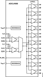
The ADCLK950 is an ultrafast clock fanout buffer fabricatedon the Analog Devices, Inc., proprietary XFCB3 silicon germanium(SiGe) bipolar process. This device is designed for high speedapplications requiring low jitter.
The device has two selectable differential inputs via the IN_SELcontrol pin. Both inputs are equipped with center tapped,differential, 100 Ω on-chip termination resistors. The inputsaccept dc-coupled LVPECL, CML, 3.3 V CMOS (single-ended),and ac-coupled 1.8 V CMOS, LVDS, and LVPECL inputs. AVREFx pin is available for biasing ac-coupled inputs.
The ADCLK950 features 10 full-swing emitter coupled logic(ECL) output drivers. For LVPECL (positive ECL) operation,bias VCC to the positive supply and VEE to ground. For ECLoperation, bias VCC to ground and VEE to the negative supply.
The output stages are designed to directly drive 800 mV eachside into 50 Ω terminated to VCC − 2 V for a total differentialoutput swing of 1.6 V.
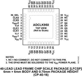
The ADCLK950 is available in a 40-lead LFCSP and specifiedfor operation over the standard industrial temperature range of−40°C to +85°C.
Applications
- Low jitter clock distribution
- Clock and data signal restoration
- Level translation
- Wireless communications
- Wired communications
- Medical and industrial imaging
- ATE and high performance instrumentation
This product has been released to the market. The data sheet contains all final specifications and operating conditions. For new designs, ADI recommends utilization of these products.


