
- Manufacturer Part Number : ADN4670BCPZ-REEL7
- Manufacturer : AD
- Description : Programmable Low Voltage 1:10 LVDS Clock Driver IC
- Series : ADN4670
- Reference Price : USD 3.8
- Our Price : We have a better price, contact us by email
- Product Type : Clock Generation & Distribution
- Function : Clock Distribution Devices
- Current Suggest : Production
- Status : Production
- ROHS Status : ROHS Compliant (Lead Free)
- Package Type : 32-Lead LFCSP (5mm x 5mm w/ EP)
- Pins : 32
- MFG Package Case : CP-32-7
- Part Type : REEL
- Standard Packing Type : Reel
- Standard Packing Quantity : 1500
- Working Temperature : -40 to 85C
- Other Part Number : ADN4670BCPZ-REEL7
- Shipping methods : DHL FEDEX UPS TNT
- Delivery Time : Ship within 1 day.
- Manufacturer Production time : 6-8 weeks (Normally have stocks)
- Weight : 0.001KG
Contact us to check the best price and real time inventory quantity for ADN4670BCPZ-REEL7. If you need any more information about ADN4670BCPZ-REEL7, you can also send us by email. Our email is [email protected], we will reply you in 12 hours.
- Low output skew <30 ps (typical)
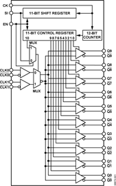
- Distributes one differential clock input to 10 LVDS clock outputs
- Programmable—one of two differential clock inputs can be selected (CLK0, CLK1) and individual differential clock outputs enabled/disabled
- Signaling rate up to 1.1 GHz (typical)
- 2.375 V to 2.625 V power supply range
- ±100 mV differential input threshold
- Input common-mode range from rail-to-rail
- I/O pins fail-safe during power-down: VDD = 0 V
- Available in 32-lead LFCSP package
- Industrial operating temperature range: −40°C to +85°C
When the enable input EN is high, the device may be pro-grammed by clocking 11 data bits into the shift register. The first 10 bits determine which outputs are enabled (0 = disabled, 1 = enabled), while the 11th bit selects the clock input (0 = CLK0, 1 = CLK1). A 12th clock pulse transfers data from the shift register to the control register.
The ADN4670 is fully specified over the industrial temperature range and is available in a 32-lead LFCSP package.
Applications
At least one model within this product family is in production and available for purchase. The product is appropriate for new designs but newer alternatives may exist.


