
- Manufacturer Part Number : DC2026C-KIT
- Manufacturer : AD
- Description : Ultralow Jitter, 4.5GHz PLL with 11 Outputs and JESD204B / JESD204C Support IC
- Series : LTC6952
- Reference Price : USD 0
- Our Price : We have a better price, contact us by email
- Product Type : Clock Generation & Distribution
- Function : Clock Generation Devices
- Current Suggest : Recommended for New Designs
- Status : Production
- ROHS Status : ROHS Compliant (Lead Free)
- Package Type : DC2026C with DC934A | Linduino One Isolated Arduino-Compatible Demonstration Board with LTC2607/LTC2422 (DC934A) Demo Board
- Pins : -
- MFG Package Case : -
- Part Type : EVAL
- Standard Packing Type : -
- Standard Packing Quantity : -
- Working Temperature : -
- Other Part Number : DC2026C-KIT
- Shipping methods : DHL FEDEX UPS TNT
- Delivery Time : Ship within 1 day.
- Manufacturer Production time : 6-8 weeks (Normally have stocks)
- Weight : 0.001KG
Contact us to check the best price and real time inventory quantity for DC2026C-KIT. If you need any more information about DC2026C-KIT, you can also send us by email. Our email is [email protected], we will reply you in 12 hours.
- JESD204B/C, Subclass 1 SYSREF Signal Generation
- Low Noise Integer-N PLL
- Additive Output Jitter < 6fsRMS
- (Integration BW = 12kHz to 20MHz, f = 4.5GHz)
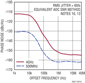
- Additive Output Jitter 65fsRMS (ADC SNR Method)
- EZSync™, ParallelSync™ Multichip Synchronization
- –229dBc/Hz Normalized In-Band Phase Noise Floor
- –281dBc/Hz Normalized In-Band 1/f Noise
- Eleven Independent, Low Noise Outputs with Programmable Coarse Digital and Fine Analog Delays
- Flexible Outputs Can Serve as Either a Device Clock or SYSREF Signal
- Reference Input Frequency up to 500MHz
- LTC6952Wizard™ Software Design Tool Support
- –40ºC to 125°C Operating Junction Temperature Range
The LTC6952 is a high performance, ultralow jitter,JESD204B/C clock generation and distribution IC. Itincludes a Phase Locked Loop (PLL) core, consisting ofa reference divider, phase-frequency detector (PFD) witha phase-lock indicator, ultralow noise charge pump andinteger feedback divider. The LTC6952’s eleven outputscan be configured as up to five JESD204B/C subclass1 device clock/SYSREF pairs plus one general purposeoutput, or simply eleven general purpose clock outputs fornon-JESD204B/C applications. Each output has its ownindividually programmable frequency divider and outputdriver. All outputs can also be synchronized and set toprecise phase alignment using individual coarse half-cycledigital delays and fine analog time delays.
For applications requiring more than eleven total outputs,multiple LTC6952s can be connected together using theEZSync or ParallelSync synchronization protocols.
Applications
- High Performance Data Converter Clocking
- Wireless Infrastructure
- Test and Measurement
This product has been released to the market. The data sheet contains all final specifications and operating conditions. For new designs, ADI recommends utilization of these products.


