
- Manufacturer Part Number : LTC6952
- Manufacturer : AD
- Description : Ultralow Jitter, 4.5GHz PLL with 11 Outputs and JESD204B / JESD204C Support
- Series : LTC6952
- Reference Price : USD 12.704
- Our Price : We have a better price, contact us by email
- Product Type : Clock Generation & Distribution
- Function : Clock Generation Devices
- Current Suggest : Recommended for New Designs
- Status : Production
- RoHS Status: -
- Voltage: -
- Feature: -
- Package Case: -
- Temperature Range: -
- Packing: Reel/Tray/Tube
- Standard Packing Quantity: -
- Country of Origin: -
- Other Part Number : LTC6952
- Shipping methods : DHL FEDEX UPS TNT
- Delivery Time : Ship within 1 day.
- Manufacturer Production time : 6-8 weeks (Normally have stocks)
- Weight : 0.001KG
Contact us to check the best price and real time inventory quantity for LTC6952. If you need any more information about LTC6952, you can also send us by email. Our email is [email protected], we will reply you in 12 hours.
- JESD204B/C, Subclass 1 SYSREF Signal Generation
- Low Noise Integer-N PLL
- Additive Output Jitter < 6fsRMS
- (Integration BW = 12kHz to 20MHz, f = 4.5GHz)
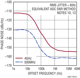
- Additive Output Jitter 65fsRMS (ADC SNR Method)
- EZSync™, ParallelSync™ Multichip Synchronization
- –229dBc/Hz Normalized In-Band Phase Noise Floor
- –281dBc/Hz Normalized In-Band 1/f Noise
- Eleven Independent, Low Noise Outputs with Programmable Coarse Digital and Fine Analog Delays
- Flexible Outputs Can Serve as Either a Device Clock or SYSREF Signal
- Reference Input Frequency up to 500MHz
- LTC6952Wizard™ Software Design Tool Support
- –40ºC to 125°C Operating Junction Temperature Range
The LTC6952 is a high performance, ultralow jitter,JESD204B/C clock generation and distribution IC. Itincludes a Phase Locked Loop (PLL) core, consisting ofa reference divider, phase-frequency detector (PFD) witha phase-lock indicator, ultralow noise charge pump andinteger feedback divider. The LTC6952’s eleven outputscan be configured as up to five JESD204B/C subclass1 device clock/SYSREF pairs plus one general purposeoutput, or simply eleven general purpose clock outputs fornon-JESD204B/C applications. Each output has its ownindividually programmable frequency divider and outputdriver. All outputs can also be synchronized and set toprecise phase alignment using individual coarse half-cycledigital delays and fine analog time delays.
For applications requiring more than eleven total outputs,multiple LTC6952s can be connected together using theEZSync or ParallelSync synchronization protocols.
Applications
- High Performance Data Converter Clocking
- Wireless Infrastructure
- Test and Measurement
This product has been released to the market. The data sheet contains all final specifications and operating conditions. For new designs, ADI recommends utilization of these products.


