
- Manufacturer Part Number : AD5313
- Manufacturer : AD
- Description : 2.5 V to 5.5 V, 230 µA, Dual Rail-to-Rail Voltage Output 10-Bit DAC
- Series : AD5313
- Reference Price : USD 2.024
- Our Price : We have a better price, contact us by email
- Product Type : Precision D/A Converters
- Function : Voltage Output D/A Converters
- Current Suggest : Production
- Status : Production
- RoHS Status: -
- Voltage: -
- Feature: -
- Package Case: -
- Temperature Range: -
- Packing: Reel/Tray/Tube
- Standard Packing Quantity: -
- Country of Origin: -
- Other Part Number : AD5313
- Shipping methods : DHL FEDEX UPS TNT
- Delivery Time : Ship within 1 day.
- Manufacturer Production time : 6-8 weeks (Normally have stocks)
- Weight : 0.001KG
Contact us to check the best price and real time inventory quantity for AD5313. If you need any more information about AD5313, you can also send us by email. Our email is [email protected], we will reply you in 12 hours.
- AD5313: 2 buffered 10-bit DACs in 1 package
A version: ±4 LSB INL
B version: ±2 LSB INL - AD5323: 2 buffered 12-bit DACs in 1 package
A version: ±16 LSB INL
B version: ±8 LSB INL - Micropower operation: 300 μA at 5 V (including reference current)
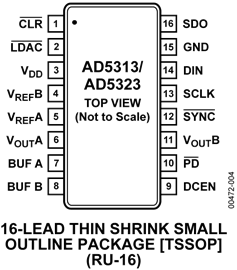
- 16-lead TSSOP package
- Power-down to 200 nA at 5 V, 50 nA at 3 V
- 2.5 V to 5.5 V power supply
- Double-buffered input logic
- Guaranteed monotonic by design over all codes
- Buffered/unbuffered reference input options
- Output range: 0 V to VREF or 0 7 V to 2 VREF
- Power-on-reset to 0 V
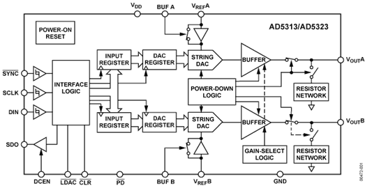
The AD5313/AD5323 are dual 8-/10-/12-bit buffered voltage output DACs in a 16-lead TSSOP package that operate from a single 2.5 V to 5.5 V supply, consuming 230 μA at 3 V. Their on-chip output amplifiers allow the outputs to swing rail-to-rail with a slew rate of 0.7 V/μs. The AD5313/AD5323 utilize a versatile 3-wire serial interface that operates at clock rates up to 30 MHz and is compatible with standard SPI, QSPI™, MICROWIRE™, and DSP interface standards.
The references for the two DACs are derived from two reference pins (one per DAC). These reference inputs may be configured as buffered or unbuffered inputs. The parts incorporate a power-on reset circuit, which ensures that the DAC outputs power up to 0 V and remain there until a valid write to the device takes place. There is also an asynchronous active low CLR pin that clears both DACs to 0 V. The outputs of both DACs may be updated simultaneously using the asynchronous LDAC input. The parts contain a power-down feature that reduces the current consumption of the devices to 200 nA at 5 V (50 nA at 3 V) and provides software-selectable output loads while in power-down mode. The parts may also be used in daisy-chaining applications using the SDO pin.
The low power consumption of these parts in normal operation makes them ideally suited to portable battery-operated equipment. The power consumption is 1.5 mW at 5 V and 0.7 mW at 3 V, reducing to 1 μW in power-down mode.
Applications
- Portable battery-powered instruments
- Digital gain and offset adjustment
- Programmable voltage and current sources
- Programmable attenuators
At least one model within this product family is in production and available for purchase. The product is appropriate for new designs but newer alternatives may exist.


