
- Manufacturer Part Number : AD5316RBCPZ-RL7
- Manufacturer : AD
- Description : Quad, 10-Bit nanoDAC with 2 ppm/°C Reference, I2C Interface IC
- Series : AD5316R
- Reference Price : USD 2.304
- Our Price : We have a better price, contact us by email
- Product Type : Precision D/A Converters
- Function : Voltage Output D/A Converters
- Current Suggest : Recommended for New Designs
- Status : Production
- ROHS Status : ROHS Compliant (Lead Free)
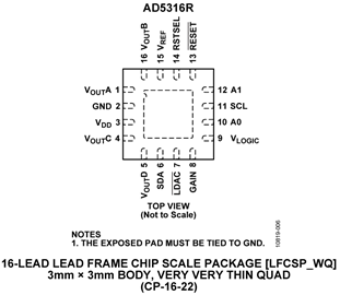
- Package Type : 16-Lead LFCSP (3mm x 3mm w/ EP)
- Pins : 16
- MFG Package Case : CP-16-22
- Part Type : REEL
- Standard Packing Type : Reel
- Standard Packing Quantity : 1500
- Working Temperature : -40 to 105C
- Other Part Number : AD5316RBCPZ-RL7
- Shipping methods : DHL FEDEX UPS TNT
- Delivery Time : Ship within 1 day.
- Manufacturer Production time : 6-8 weeks (Normally have stocks)
- Weight : 0.001KG
Contact us to check the best price and real time inventory quantity for AD5316RBCPZ-RL7. If you need any more information about AD5316RBCPZ-RL7, you can also send us by email. Our email is [email protected], we will reply you in 12 hours.
- Low drift 2.5 V on-chip reference: 2 ppm/°C typical
- Tiny package: 3 mm × 3 mm, 16-lead LFCSP
- TUE: ±0.1% of FSR maximum
- Offset error: ±1.5 mV maximum
- Gain error: ±0.1% of FSR maximum
- High drive capability: 20 mA, 0.5 V from supply rails
- User-selectable gain of 1 or 2 (GAIN pin)
- Reset to zero scale or midscale (RSTSEL pin)
- 1.8 V logic compatibility
- 400 kHz I2C-compatible serial interface
- 4 I2C addresses available
- Low glitch: 0.5 nV-sec
- Low power: 3.3 mW at 3 V
- 2.7 V to 5.5 V power supply
- −40°C to +105°C temperature range
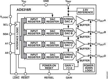
The AD5316R, a member of the nanoDAC® family, is a low power,quad, 10-bit buffered voltage output DAC. The device includesa 2.5 V, 2 ppm/°C internal reference (enabled by default) and again select pin giving a full-scale output of 2.5 V (gain = 1) or 5 V(gain = 2). The device operates from a single 2.7 V to 5.5 V supply,is guaranteed monotonic by design, and exhibits less than 0.1%FSR gain error and 1.5 mV offset error performance. The device is available in a 3 mm × 3 mm lead lead frame chip scale package (LFCSP) and in a thin shrink small outline package (TSSOP).
The AD5316R also incorporates a power-on reset circuit and aRSTSEL pin. The RSTSEL pin ensures that the DAC outputs powerup to zero scale or midscale and remain at that level until a validwrite takes place. The device contains a per channel power-down feature that reduces the current consumption of the device in power-down mode to 4 μA at 3 V.
The AD5316R uses a versatile 2-wire serial interface that operatesat clock rates up to 400 kHz and includes a VLOGIC pin intendedfor 1.8 V/3 V/5 V logic.
Product Highlights- Precision DC Performance.
Total unadjusted error (TUE): ±0.1% of FSR maximum
Offset error: ±1.5 mV maximum
Gain error: ±0.1% of FSR maximum - Low Drift 2.5 V On-Chip Reference.
2 ppm/°C typical temperature coefficient
5 ppm/°C maximum temperature coefficient - Two Package Options.
3 mm × 3 mm, 16-lead LFCSP
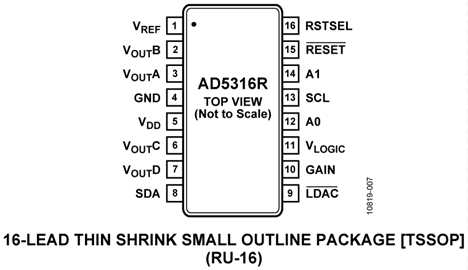
16-lead TSSOP
Applications
- Digital gain and offset adjustment
- Programmable attenuators
- Industrial automation
- Data acquisition systems
This product has been released to the market. The data sheet contains all final specifications and operating conditions. For new designs, ADI recommends utilization of these products.


