
- Manufacturer Part Number : AD5316R
- Manufacturer : AD
- Description : Quad, 10-Bit nanoDAC with 2 ppm/°C Reference, I2C Interface
- Series : AD5316R
- Reference Price : USD 2.304
- Our Price : We have a better price, contact us by email
- Product Type : Precision D/A Converters
- Function : Voltage Output D/A Converters
- Current Suggest : Recommended for New Designs
- Status : Production
- RoHS Status: -
- Voltage: -
- Feature: -
- Package Case: -
- Temperature Range: -
- Packing: Reel/Tray/Tube
- Standard Packing Quantity: -
- Country of Origin: -
- Other Part Number : AD5316R
- Shipping methods : DHL FEDEX UPS TNT
- Delivery Time : Ship within 1 day.
- Manufacturer Production time : 6-8 weeks (Normally have stocks)
- Weight : 0.001KG
Contact us to check the best price and real time inventory quantity for AD5316R. If you need any more information about AD5316R, you can also send us by email. Our email is [email protected], we will reply you in 12 hours.
- Low drift 2.5 V on-chip reference: 2 ppm/°C typical
- Tiny package: 3 mm × 3 mm, 16-lead LFCSP
- TUE: ±0.1% of FSR maximum
- Offset error: ±1.5 mV maximum
- Gain error: ±0.1% of FSR maximum
- High drive capability: 20 mA, 0.5 V from supply rails
- User-selectable gain of 1 or 2 (GAIN pin)
- Reset to zero scale or midscale (RSTSEL pin)
- 1.8 V logic compatibility
- 400 kHz I2C-compatible serial interface
- 4 I2C addresses available
- Low glitch: 0.5 nV-sec
- Low power: 3.3 mW at 3 V
- 2.7 V to 5.5 V power supply
- −40°C to +105°C temperature range
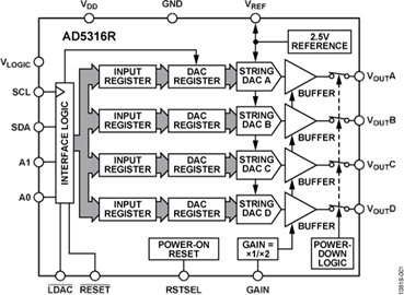
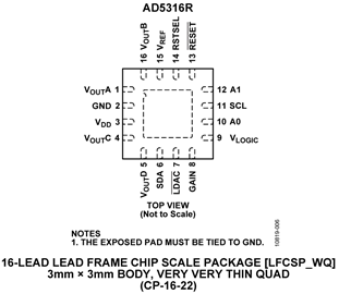
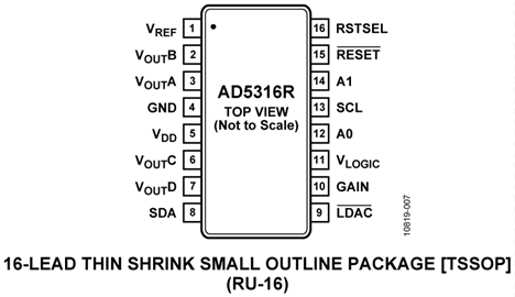
The AD5316R, a member of the nanoDAC® family, is a low power,quad, 10-bit buffered voltage output DAC. The device includesa 2.5 V, 2 ppm/°C internal reference (enabled by default) and again select pin giving a full-scale output of 2.5 V (gain = 1) or 5 V(gain = 2). The device operates from a single 2.7 V to 5.5 V supply,is guaranteed monotonic by design, and exhibits less than 0.1%FSR gain error and 1.5 mV offset error performance. The device is available in a 3 mm × 3 mm lead lead frame chip scale package (LFCSP) and in a thin shrink small outline package (TSSOP).
The AD5316R also incorporates a power-on reset circuit and aRSTSEL pin. The RSTSEL pin ensures that the DAC outputs powerup to zero scale or midscale and remain at that level until a validwrite takes place. The device contains a per channel power-down feature that reduces the current consumption of the device in power-down mode to 4 μA at 3 V.
The AD5316R uses a versatile 2-wire serial interface that operatesat clock rates up to 400 kHz and includes a VLOGIC pin intendedfor 1.8 V/3 V/5 V logic.
Product Highlights- Precision DC Performance.
Total unadjusted error (TUE): ±0.1% of FSR maximum
Offset error: ±1.5 mV maximum
Gain error: ±0.1% of FSR maximum - Low Drift 2.5 V On-Chip Reference.
2 ppm/°C typical temperature coefficient
5 ppm/°C maximum temperature coefficient - Two Package Options.
3 mm × 3 mm, 16-lead LFCSP
16-lead TSSOP
Applications
- Digital gain and offset adjustment
- Programmable attenuators
- Industrial automation
- Data acquisition systems
This product has been released to the market. The data sheet contains all final specifications and operating conditions. For new designs, ADI recommends utilization of these products.


