
- Manufacturer Part Number : AD5348BCPZ
- Manufacturer : AD
- Description : 2.5 V to 5.5 V, Parallel Interface Octal Voltage Output 12-Bit D/A Converter IC
- Series : AD5348
- Reference Price : USD 8.24
- Our Price : We have a better price, contact us by email
- Product Type : Precision D/A Converters
- Function : Voltage Output D/A Converters
- Current Suggest : Production
- Status : Production
- ROHS Status : ROHS Compliant (Lead Free)
- Package Type : 40-Lead LFCSP (6mm x 6mm w/ EP)
- Pins : 40
- MFG Package Case : CP-40-9
- Part Type : OTH
- Standard Packing Type : Tray
- Standard Packing Quantity : 490
- Working Temperature : -40 to 105C
- Other Part Number : AD5348BCPZ
- Shipping methods : DHL FEDEX UPS TNT
- Delivery Time : Ship within 1 day.
- Manufacturer Production time : 6-8 weeks (Normally have stocks)
- Weight : 0.001KG
Contact us to check the best price and real time inventory quantity for AD5348BCPZ. If you need any more information about AD5348BCPZ, you can also send us by email. Our email is [email protected], we will reply you in 12 hours.
- Low power operation: 1.4 mA (max) at 3.6 V
- Power-down to 120 nA at 3 V, 400 nA at 5 V
- Guaranteed monotonic by design over all codes
- Rail-to-rail output range:
0 V to VREF or 0 V to 2 × VREF - Power-on reset to 0 V
- Simultaneous update of DAC outputs via LDAC pin
- Asynchronous CLR facility
- Readback
- Buffered/unbuffered reference inputs
- 20 ns WR time
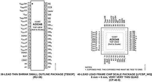
- 38-lead TSSOP/6 mm × 6 mm 40-lead LFCSP packaging
- Temperature range: –40°C to +105°C
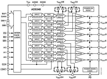
The AD5346/AD5347/AD5348 are octal 8-, 10-, and 12- bit DACs, operating from a 2.5 V to 5.5 V supply. These devices incorporate an on-chip output buffer that can drive the output to both supply rails, and also allows a choice of buffered or unbuffered reference input.
The AD5346/AD5347/AD5348 have a parallel interface. CS selects the device and data is loaded into the input registers on the rising edge of WR. A readback feature allows the internal DAC registers to be read back through the digital port.
The GAIN pin on these devices allows the output range to be set at 0 V to VREF or 0 V to 2 x VREF.
Input data to the DACs is double-buffered, allowing simultaneous update of multiple DACs in a system using the LDAC pin.
An asynchronous CLR input is also provided, which resets the contents of the Input Register and the DAC Register to all zeros. These devices also incorporate a power-on-reset circuit that ensures that the DAC output powers on to 0 V and remains there until valid data is written to the device. All three parts are pin-compatible, which allows the user to select the amount of resolution appropriate for their application without redesigning their circuit board.
APPLICATIONS
- Portable battery-powered instruments
- Digital gain and offset adjustment
- Programmable voltage and current sources
- Optical networking
- Automatic test equipment
- Mobile communications
- Programmable attenuators
- Industrial process control
At least one model within this product family is in production and available for purchase. The product is appropriate for new designs but newer alternatives may exist.


