
- Manufacturer Part Number : AD5790BCPZ-RL7
- Manufacturer : AD
- Description : System Ready 20-Bit, ±2 LSB INL, Voltage Output DAC IC
- Series : AD5790
- Reference Price : USD 54
- Our Price : We have a better price, contact us by email
- Product Type : Precision D/A Converters
- Function : Voltage Output D/A Converters
- Current Suggest : Recommended for New Designs
- Status : Production
- ROHS Status : ROHS Compliant (Lead Free)
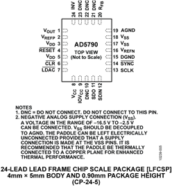
- Package Type : 24-Lead LFCSP (4mm x 5mm w/ EP)
- Pins : 24
- MFG Package Case : CP-24-5
- Part Type : REEL
- Standard Packing Type : Reel
- Standard Packing Quantity : 1500
- Working Temperature : -40 to 125C
- Other Part Number : AD5790BCPZ-RL7
- Shipping methods : DHL FEDEX UPS TNT
- Delivery Time : Ship within 1 day.
- Manufacturer Production time : 6-8 weeks (Normally have stocks)
- Weight : 0.001KG
Contact us to check the best price and real time inventory quantity for AD5790BCPZ-RL7. If you need any more information about AD5790BCPZ-RL7, you can also send us by email. Our email is [email protected], we will reply you in 12 hours.
- Single 20-bit voltage output DAC, ±2 LSB INL
- 8 nV/√Hz output noise spectral density
- 0.1 LSB long term linearity error stability
- ±0.018 ppm/°C gain error temperature coefficient
- 2.5 µs output voltage settling time
- 3.5 nV-sec midscale glitch impulse
- Integrated Precision Reference Buffers
- Operating temperature range: −40°C to +125°C
- 4mm x 5mm LFCSP package
- Wide power supply range of up to ±16.5 V
- 35 MHz Schmitt-triggered digital interface
- 1.8 V compatible digital interface
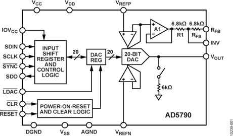
The AD57901 is a single 20-bit, voltage out Dac that operates from a bipolar supply up to 33V. Reference buffers are also provided on-chip The AD5790 accepts a positive reference input in the range of 5V to VDD – 2.5V and a negative reference input in the range of VSS + 2.5v to 0V. The AD5790 offers a relative accuracy of +/-2 LSB's max and operation is guaranteed monotonic with a -1 LSB to +3 LSB's DNL specification.
The part uses a versatile 3-wire serial interface that operates at clock rates up to 35 MHz and is compatible with standard SPI®, QSPI™, MICROWIRE™, and DSP interface standards. The part incorporates a power-on reset circuit that ensures the DAC output powers up to 0V and in a known output impedance state and remains in this state until a valid write to the device takes place. The part provides a disable feature that places the output in a defined load state.
1Protected by U.S. Patent No. 7,884,747 and 8,089,380
Product Highlights
- 20-bit resolution
- Wide power supply range of up to ±16.5 V.
- −40°C to +125°C operating temperature range.
- Low 8 nV/√Hz noise.
- Low ±0.018 ppm/°C gain error temperature coefficient.
Applications
- Medical instrumentation
- Test and measurement
- Industrial control
- Scientific and aerospace instrumentation
- Data acquisition systems
- Digital gain and offset adjustment
- Power supply control
This product has been released to the market. The data sheet contains all final specifications and operating conditions. For new designs, ADI recommends utilization of these products.


