
- Manufacturer Part Number : AD5790
- Manufacturer : AD
- Description : System Ready 20-Bit, ±2 LSB INL, Voltage Output DAC
- Series : AD5790
- Reference Price : USD 54
- Our Price : We have a better price, contact us by email
- Product Type : Precision D/A Converters
- Function : Voltage Output D/A Converters
- Current Suggest : Recommended for New Designs
- Status : Production
- RoHS Status: -
- Voltage: -
- Feature: -
- Package Case: -
- Temperature Range: -
- Packing: Reel/Tray/Tube
- Standard Packing Quantity: -
- Country of Origin: -
- Other Part Number : AD5790
- Shipping methods : DHL FEDEX UPS TNT
- Delivery Time : Ship within 1 day.
- Manufacturer Production time : 6-8 weeks (Normally have stocks)
- Weight : 0.001KG
Contact us to check the best price and real time inventory quantity for AD5790. If you need any more information about AD5790, you can also send us by email. Our email is [email protected], we will reply you in 12 hours.
- Single 20-bit voltage output DAC, ±2 LSB INL
- 8 nV/√Hz output noise spectral density
- 0.1 LSB long term linearity error stability
- ±0.018 ppm/°C gain error temperature coefficient
- 2.5 µs output voltage settling time
- 3.5 nV-sec midscale glitch impulse
- Integrated Precision Reference Buffers
- Operating temperature range: −40°C to +125°C
- 4mm x 5mm LFCSP package
- Wide power supply range of up to ±16.5 V
- 35 MHz Schmitt-triggered digital interface
- 1.8 V compatible digital interface
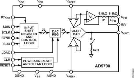
The AD57901 is a single 20-bit, voltage out Dac that operates from a bipolar supply up to 33V. Reference buffers are also provided on-chip The AD5790 accepts a positive reference input in the range of 5V to VDD – 2.5V and a negative reference input in the range of VSS + 2.5v to 0V. The AD5790 offers a relative accuracy of +/-2 LSB's max and operation is guaranteed monotonic with a -1 LSB to +3 LSB's DNL specification.
The part uses a versatile 3-wire serial interface that operates at clock rates up to 35 MHz and is compatible with standard SPI®, QSPI™, MICROWIRE™, and DSP interface standards. The part incorporates a power-on reset circuit that ensures the DAC output powers up to 0V and in a known output impedance state and remains in this state until a valid write to the device takes place. The part provides a disable feature that places the output in a defined load state.
1Protected by U.S. Patent No. 7,884,747 and 8,089,380
Product Highlights
- 20-bit resolution
- Wide power supply range of up to ±16.5 V.
- −40°C to +125°C operating temperature range.
- Low 8 nV/√Hz noise.
- Low ±0.018 ppm/°C gain error temperature coefficient.
Applications
- Medical instrumentation
- Test and measurement
- Industrial control
- Scientific and aerospace instrumentation
- Data acquisition systems
- Digital gain and offset adjustment
- Power supply control
This product has been released to the market. The data sheet contains all final specifications and operating conditions. For new designs, ADI recommends utilization of these products.


